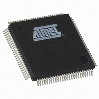
AT91SAM7A3-AU Atmel, AT91SAM7A3-AU Datasheet - Page 323

AT91SAM7A3-AU
Manufacturer Part Number
AT91SAM7A3-AU
Description
IC ARM7 MCU FLASH 256K 100LQFP
Manufacturer
Atmel
Series
AT91SAMr
Specifications of AT91SAM7A3-AU
Core Processor
ARM7
Core Size
16/32-Bit
Speed
60MHz
Connectivity
CAN, I²C, MMC, SPI, SSC, UART/USART
Peripherals
POR, PWM, WDT
Number Of I /o
62
Program Memory Size
256KB (256K x 8)
Program Memory Type
FLASH
Ram Size
32K x 8
Voltage - Supply (vcc/vdd)
1.65 V ~ 1.95 V
Data Converters
A/D 8x10b
Oscillator Type
Internal
Operating Temperature
-40°C ~ 85°C
Package / Case
100-LQFP
Controller Family/series
AT91SAM7xx
No. Of I/o's
62
Ram Memory Size
32KB
Cpu Speed
60MHz
No. Of Timers
3
Rohs Compliant
Yes
Package
100LQFP
Device Core
ARM7TDMI
Family Name
91S
Maximum Speed
60 MHz
Operating Supply Voltage
3.3 V
Data Bus Width
32 Bit
Number Of Programmable I/os
62
Interface Type
CAN/SPI/I2S/TWI/USART/USB
On-chip Adc
2(8-chx10-bit)
Number Of Timers
3
Processor Series
AT91SAMx
Core
ARM7TDMI
Data Ram Size
32 KB
Maximum Clock Frequency
60 MHz
Maximum Operating Temperature
+ 85 C
Mounting Style
SMD/SMT
3rd Party Development Tools
JTRACE-ARM-2M, MDK-ARM, RL-ARM, ULINK2
Development Tools By Supplier
AT91SAM-ICE, AT91-ISP, AT91SAM7A3-EK
Minimum Operating Temperature
- 40 C
Cpu Family
91S
Device Core Size
32b
Frequency (max)
60MHz
Total Internal Ram Size
32KB
# I/os (max)
62
Number Of Timers - General Purpose
3
Operating Supply Voltage (typ)
3.3V
Operating Supply Voltage (max)
3.6V
Operating Supply Voltage (min)
3V
Instruction Set Architecture
RISC
Operating Temp Range
-40C to 85C
Operating Temperature Classification
Industrial
Mounting
Surface Mount
Pin Count
100
Package Type
LQFP
For Use With
AT91SAM-ICE - EMULATOR FOR AT91 ARM7/ARM9AT91SAM7A3-EK - KIT EVAL FOR AT91SAM7A3
Lead Free Status / RoHS Status
Lead free / RoHS Compliant
Eeprom Size
-
Lead Free Status / Rohs Status
Details
Available stocks
Company
Part Number
Manufacturer
Quantity
Price
Company:
Part Number:
AT91SAM7A3-AU
Manufacturer:
MXIC
Quantity:
1 001
Company:
Part Number:
AT91SAM7A3-AU
Manufacturer:
Atmel
Quantity:
730
- Current page: 323 of 594
- Download datasheet (7Mb)
30.6.1.4
30.6.2
6042E–ATARM–14-Dec-06
Transmitter Operations
Serial Clock Ratio Considerations
Figure 30-7. Receiver Clock Management
The Transmitter and the Receiver can be programmed to operate with the clock signals pro-
vided on either the TK or RK pins. This allows the SSC to support many slave-mode data
transfers. In this case, the maximum clock speed allowed on the RK pin is:
In addition, the maximum clock speed allowed on the TK pin is:
A transmitted frame is triggered by a start event and can be followed by synchronization data
before data transmission.
The start event is configured by setting the Transmit Clock Mode Register (SSC_TCMR).
“Start” on page 325.
The frame synchronization is configured setting the Transmit Frame Mode Register
(SSC_TFMR).
To transmit data, the transmitter uses a shift register clocked by the transmitter clock signal
and the start mode selected in the SSC_TCMR. Data is written by the application to the
SSC_THR register then transferred to the shift register according to the data format selected.
When both the SSC_THR and the transmit shift register are empty, the status flag TXEMPTY
is set in SSC_SR. When the Transmit Holding register is transferred in the Transmit shift reg-
ister, the status flag TXRDY is set in SSC_SR and additional data can be loaded in the holding
register.
– Master Clock divided by 2 if Receiver Frame Synchro is input
– Master Clock divided by 3 if Receiver Frame Synchro is output
– Master Clock divided by 6 if Transmit Frame Synchro is input
– Master Clock divided by 2 if Transmit Frame Synchro is output
Transmitter
RK (pin)
Divider
Clock
Clock
See “Frame Sync” on page 327.
MUX
CKS
CKO
AT91SAM7A3 Preliminary
Controller
Tri-state
MUX
INV
CKI
Data Transfer
Controller
Tri-state
CKG
Receiver
Clock
Clock
Output
See
323
Related parts for AT91SAM7A3-AU
Image
Part Number
Description
Manufacturer
Datasheet
Request
R

Part Number:
Description:
MCU ARM9 64K SRAM 144-LFBGA
Manufacturer:
Atmel
Datasheet:

Part Number:
Description:
IC ARM9 MPU 217-LFBGA
Manufacturer:
Atmel
Datasheet:

Part Number:
Description:
MCU ARM9 ULTRA LOW PWR 217-LFBGA
Manufacturer:
Atmel
Datasheet:

Part Number:
Description:
MCU ARM9 324-TFBGA
Manufacturer:
Atmel
Datasheet:

Part Number:
Description:
IC MCU ARM9 SAMPLING 217CBGA
Manufacturer:
Atmel
Datasheet:

Part Number:
Description:
IC ARM9 MCU 217-LFBGA
Manufacturer:
Atmel
Datasheet:

Part Number:
Description:
IC ARM9 MCU 208-PQFP
Manufacturer:
Atmel
Datasheet:

Part Number:
Description:
MCU ARM 512K HS FLASH 100-LQFP
Manufacturer:
Atmel
Datasheet:

Part Number:
Description:
MCU ARM 512K HS FLASH 100-TFBGA
Manufacturer:
Atmel
Datasheet:

Part Number:
Description:
IC ARM9 MCU 200 MHZ 324-TFBGA
Manufacturer:
Atmel
Datasheet:

Part Number:
Description:
IC ARM MCU 16BIT 128K 256BGA
Manufacturer:
Atmel
Datasheet:

Part Number:
Description:
IC ARM7 MCU 32BIT 128K 64LQFP
Manufacturer:
Atmel
Datasheet:

Part Number:
Description:
IC ARM7 MCU FLASH 256K 128-LQFP
Manufacturer:
Atmel
Datasheet:

Part Number:
Description:
IC ARM7 MCU FLASH 512K 128-LQFP
Manufacturer:
Atmel
Datasheet:

Part Number:
Description:
IC ARM9 MPU 217-LFBGA
Manufacturer:
Atmel
Datasheet:


