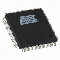
AT91SAM7A3-AU Atmel, AT91SAM7A3-AU Datasheet - Page 422

AT91SAM7A3-AU
Manufacturer Part Number
AT91SAM7A3-AU
Description
IC ARM7 MCU FLASH 256K 100LQFP
Manufacturer
Atmel
Series
AT91SAMr
Specifications of AT91SAM7A3-AU
Core Processor
ARM7
Core Size
16/32-Bit
Speed
60MHz
Connectivity
CAN, I²C, MMC, SPI, SSC, UART/USART
Peripherals
POR, PWM, WDT
Number Of I /o
62
Program Memory Size
256KB (256K x 8)
Program Memory Type
FLASH
Ram Size
32K x 8
Voltage - Supply (vcc/vdd)
1.65 V ~ 1.95 V
Data Converters
A/D 8x10b
Oscillator Type
Internal
Operating Temperature
-40°C ~ 85°C
Package / Case
100-LQFP
Controller Family/series
AT91SAM7xx
No. Of I/o's
62
Ram Memory Size
32KB
Cpu Speed
60MHz
No. Of Timers
3
Rohs Compliant
Yes
Package
100LQFP
Device Core
ARM7TDMI
Family Name
91S
Maximum Speed
60 MHz
Operating Supply Voltage
3.3 V
Data Bus Width
32 Bit
Number Of Programmable I/os
62
Interface Type
CAN/SPI/I2S/TWI/USART/USB
On-chip Adc
2(8-chx10-bit)
Number Of Timers
3
Processor Series
AT91SAMx
Core
ARM7TDMI
Data Ram Size
32 KB
Maximum Clock Frequency
60 MHz
Maximum Operating Temperature
+ 85 C
Mounting Style
SMD/SMT
3rd Party Development Tools
JTRACE-ARM-2M, MDK-ARM, RL-ARM, ULINK2
Development Tools By Supplier
AT91SAM-ICE, AT91-ISP, AT91SAM7A3-EK
Minimum Operating Temperature
- 40 C
Cpu Family
91S
Device Core Size
32b
Frequency (max)
60MHz
Total Internal Ram Size
32KB
# I/os (max)
62
Number Of Timers - General Purpose
3
Operating Supply Voltage (typ)
3.3V
Operating Supply Voltage (max)
3.6V
Operating Supply Voltage (min)
3V
Instruction Set Architecture
RISC
Operating Temp Range
-40C to 85C
Operating Temperature Classification
Industrial
Mounting
Surface Mount
Pin Count
100
Package Type
LQFP
For Use With
AT91SAM-ICE - EMULATOR FOR AT91 ARM7/ARM9AT91SAM7A3-EK - KIT EVAL FOR AT91SAM7A3
Lead Free Status / RoHS Status
Lead free / RoHS Compliant
Eeprom Size
-
Lead Free Status / Rohs Status
Details
Available stocks
Company
Part Number
Manufacturer
Quantity
Price
Company:
Part Number:
AT91SAM7A3-AU
Manufacturer:
MXIC
Quantity:
1 001
Company:
Part Number:
AT91SAM7A3-AU
Manufacturer:
Atmel
Quantity:
730
- Current page: 422 of 594
- Download datasheet (7Mb)
33.5.2.7
422
AT91SAM7A3 Preliminary
Using Endpoints With Ping-pong Attributes
During isochronous transfer, using an endpoint with ping-pong attributes is obligatory. To be
able to guarantee a constant bandwidth, the microcontroller must read the previous data pay-
load sent by the host, while the current data payload is received by the USB device. Thus two
banks of memory are used. While one is available for the microcontroller, the other one is locked
by the USB device.
Figure 33-10. Bank Swapping in Data OUT Transfers for Ping-pong Endpoints
When using a ping-pong endpoint, the following procedures are required to perform Data OUT
transactions:
1. The host generates a Data OUT packet.
2. This packet is received by the USB device endpoint. It is written in the endpoint’s FIFO
3. The USB device sends an ACK PID packet to the host. The host can immediately send
4. The microcontroller is notified that the USB device has received a data payload, polling
5. The number of bytes available in the FIFO is made available by reading RXBYTECNT
6. The microcontroller transfers out data received from the endpoint’s memory to the
7. The microcontroller notifies the USB peripheral device that it has finished the transfer
8. A third Data OUT packet can be accepted by the USB peripheral device and copied in
9. If a second Data OUT packet has been received, the microcontroller is notified by the
Bank 0.
a second Data OUT packet. It is accepted by the device and copied to FIFO Bank 1.
RX_DATA_BK0 in the endpoint’s UDP_ CSRx register. An interrupt is pending for this
endpoint while RX_DATA_BK0 is set.
in the endpoint’s UDP_ CSRx register.
microcontroller’s memory. Data received is made available by reading the endpoint’s
UDP_ FDRx register.
by clearing RX_DATA_BK0 in the endpoint’s UDP_ CSRx register.
the FIFO Bank 0.
flag RX_DATA_BK1 set in the endpoint’s UDP_ CSRx register. An interrupt is pending
for this endpoint while RX_DATA_BK1 is set.
1 st Data Payload
2 nd Data Payload
3 rd Data Payload
Microcontroller
Write and Read at the Same Time
Bank 0
Endpoint 1
Bank 1
Endpoint 1
Bank 0
Endpoint 1
Write
USB Device
Bank 0
Endpoint 1
Bank 1
Endpoint 1
Bank 0
Endpoint 1
Read
USB Bus
2 nd Data Payload
3 rd Data Payload
1 st Data Payload
Data IN Packet
Data IN Packet
Data IN Packet
6042E–ATARM–14-Dec-06
Related parts for AT91SAM7A3-AU
Image
Part Number
Description
Manufacturer
Datasheet
Request
R

Part Number:
Description:
MCU ARM9 64K SRAM 144-LFBGA
Manufacturer:
Atmel
Datasheet:

Part Number:
Description:
IC ARM9 MPU 217-LFBGA
Manufacturer:
Atmel
Datasheet:

Part Number:
Description:
MCU ARM9 ULTRA LOW PWR 217-LFBGA
Manufacturer:
Atmel
Datasheet:

Part Number:
Description:
MCU ARM9 324-TFBGA
Manufacturer:
Atmel
Datasheet:

Part Number:
Description:
IC MCU ARM9 SAMPLING 217CBGA
Manufacturer:
Atmel
Datasheet:

Part Number:
Description:
IC ARM9 MCU 217-LFBGA
Manufacturer:
Atmel
Datasheet:

Part Number:
Description:
IC ARM9 MCU 208-PQFP
Manufacturer:
Atmel
Datasheet:

Part Number:
Description:
MCU ARM 512K HS FLASH 100-LQFP
Manufacturer:
Atmel
Datasheet:

Part Number:
Description:
MCU ARM 512K HS FLASH 100-TFBGA
Manufacturer:
Atmel
Datasheet:

Part Number:
Description:
IC ARM9 MCU 200 MHZ 324-TFBGA
Manufacturer:
Atmel
Datasheet:

Part Number:
Description:
IC ARM MCU 16BIT 128K 256BGA
Manufacturer:
Atmel
Datasheet:

Part Number:
Description:
IC ARM7 MCU 32BIT 128K 64LQFP
Manufacturer:
Atmel
Datasheet:

Part Number:
Description:
IC ARM7 MCU FLASH 256K 128-LQFP
Manufacturer:
Atmel
Datasheet:

Part Number:
Description:
IC ARM7 MCU FLASH 512K 128-LQFP
Manufacturer:
Atmel
Datasheet:

Part Number:
Description:
IC ARM9 MPU 217-LFBGA
Manufacturer:
Atmel
Datasheet:


