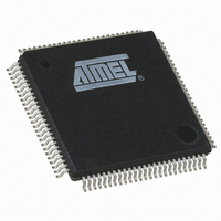
AT91SAM7A3-AU Atmel, AT91SAM7A3-AU Datasheet - Page 429

AT91SAM7A3-AU
Manufacturer Part Number
AT91SAM7A3-AU
Description
IC ARM7 MCU FLASH 256K 100LQFP
Manufacturer
Atmel
Series
AT91SAMr
Specifications of AT91SAM7A3-AU
Core Processor
ARM7
Core Size
16/32-Bit
Speed
60MHz
Connectivity
CAN, I²C, MMC, SPI, SSC, UART/USART
Peripherals
POR, PWM, WDT
Number Of I /o
62
Program Memory Size
256KB (256K x 8)
Program Memory Type
FLASH
Ram Size
32K x 8
Voltage - Supply (vcc/vdd)
1.65 V ~ 1.95 V
Data Converters
A/D 8x10b
Oscillator Type
Internal
Operating Temperature
-40°C ~ 85°C
Package / Case
100-LQFP
Controller Family/series
AT91SAM7xx
No. Of I/o's
62
Ram Memory Size
32KB
Cpu Speed
60MHz
No. Of Timers
3
Rohs Compliant
Yes
Package
100LQFP
Device Core
ARM7TDMI
Family Name
91S
Maximum Speed
60 MHz
Operating Supply Voltage
3.3 V
Data Bus Width
32 Bit
Number Of Programmable I/os
62
Interface Type
CAN/SPI/I2S/TWI/USART/USB
On-chip Adc
2(8-chx10-bit)
Number Of Timers
3
Processor Series
AT91SAMx
Core
ARM7TDMI
Data Ram Size
32 KB
Maximum Clock Frequency
60 MHz
Maximum Operating Temperature
+ 85 C
Mounting Style
SMD/SMT
3rd Party Development Tools
JTRACE-ARM-2M, MDK-ARM, RL-ARM, ULINK2
Development Tools By Supplier
AT91SAM-ICE, AT91-ISP, AT91SAM7A3-EK
Minimum Operating Temperature
- 40 C
Cpu Family
91S
Device Core Size
32b
Frequency (max)
60MHz
Total Internal Ram Size
32KB
# I/os (max)
62
Number Of Timers - General Purpose
3
Operating Supply Voltage (typ)
3.3V
Operating Supply Voltage (max)
3.6V
Operating Supply Voltage (min)
3V
Instruction Set Architecture
RISC
Operating Temp Range
-40C to 85C
Operating Temperature Classification
Industrial
Mounting
Surface Mount
Pin Count
100
Package Type
LQFP
For Use With
AT91SAM-ICE - EMULATOR FOR AT91 ARM7/ARM9AT91SAM7A3-EK - KIT EVAL FOR AT91SAM7A3
Lead Free Status / RoHS Status
Lead free / RoHS Compliant
Eeprom Size
-
Lead Free Status / Rohs Status
Details
Available stocks
Company
Part Number
Manufacturer
Quantity
Price
Company:
Part Number:
AT91SAM7A3-AU
Manufacturer:
MXIC
Quantity:
1 001
Company:
Part Number:
AT91SAM7A3-AU
Manufacturer:
Atmel
Quantity:
730
- Current page: 429 of 594
- Download datasheet (7Mb)
33.6
WARNING: The UDP peripheral clock in the Power Management Controller (PMC) must be enabled before any read/write
operations to the UDP registers including the UDP_TXCV register.
Table 33-4.
Notes:
6042E–ATARM–14-Dec-06
Offset
0x000
0x004
0x008
0x00C
0x010
0x014
0x018
0x01C
0x020
0x024
0x028
0x02C
0x030
.
.
.
See Note:
0x050
.
.
.
See Note:
0x070
0x074
0x078 - 0xFC
USB Device Port (UDP) User Interface
1. The addresses of the UDP_ CSRx registers are calculated as: 0x030 + 4(Endpoint Number - 1).
2. The addresses of the UDP_ FDRx registers are calculated as: 0x050 + 4(Endpoint Number - 1).
3. See Warning above the
(1)
(2)
UDP Memory Map
Register
Frame Number Register
Global State Register
Function Address Register
Reserved
Interrupt Enable Register
Interrupt Disable Register
Interrupt Mask Register
Interrupt Status Register
Interrupt Clear Register
Reserved
Reset Endpoint Register
Reserved
Endpoint 0 Control and Status Register
.
.
.
Endpoint 5 Control and Status Register
Endpoint 0 FIFO Data Register
.
.
.
Endpoint 5 FIFO Data Register
Reserved
Transceiver Control Register
Reserved
”UDP Memory Map”
on this page.
Name
UDP_ FRM_NUM
UDP_ GLB_STAT
UDP_ FADDR
–
UDP_ IER
UDP_ IDR
UDP_ IMR
UDP_ ISR
UDP_ ICR
–
UDP_ RST_EP
–
UDP_CSR0
UDP_CSR5
UDP_ FDR0
UDP_ FDR5
–
UDP_ TXVC
–
AT91SAM7A3 Preliminary
(3)
Access
Read
Read/Write
Read/Write
–
Write
Write
Read
Read
Write
–
Read/Write
–
Read/Write
Read/Write
Read/Write
Read/Write
–
Read/Write
–
0x0000_0000
0x0000_0100
0x0000_1200
Reset State
0x0000_0000
–
0x0000_XX00
–
–
0x0000_0000
0x0000_0000
0x0000_0000
0x0000_0000
–
0x0000_0000
–
429
Related parts for AT91SAM7A3-AU
Image
Part Number
Description
Manufacturer
Datasheet
Request
R

Part Number:
Description:
MCU ARM9 64K SRAM 144-LFBGA
Manufacturer:
Atmel
Datasheet:

Part Number:
Description:
IC ARM9 MPU 217-LFBGA
Manufacturer:
Atmel
Datasheet:

Part Number:
Description:
MCU ARM9 ULTRA LOW PWR 217-LFBGA
Manufacturer:
Atmel
Datasheet:

Part Number:
Description:
MCU ARM9 324-TFBGA
Manufacturer:
Atmel
Datasheet:

Part Number:
Description:
IC MCU ARM9 SAMPLING 217CBGA
Manufacturer:
Atmel
Datasheet:

Part Number:
Description:
IC ARM9 MCU 217-LFBGA
Manufacturer:
Atmel
Datasheet:

Part Number:
Description:
IC ARM9 MCU 208-PQFP
Manufacturer:
Atmel
Datasheet:

Part Number:
Description:
MCU ARM 512K HS FLASH 100-LQFP
Manufacturer:
Atmel
Datasheet:

Part Number:
Description:
MCU ARM 512K HS FLASH 100-TFBGA
Manufacturer:
Atmel
Datasheet:

Part Number:
Description:
IC ARM9 MCU 200 MHZ 324-TFBGA
Manufacturer:
Atmel
Datasheet:

Part Number:
Description:
IC ARM MCU 16BIT 128K 256BGA
Manufacturer:
Atmel
Datasheet:

Part Number:
Description:
IC ARM7 MCU 32BIT 128K 64LQFP
Manufacturer:
Atmel
Datasheet:

Part Number:
Description:
IC ARM7 MCU FLASH 256K 128-LQFP
Manufacturer:
Atmel
Datasheet:

Part Number:
Description:
IC ARM7 MCU FLASH 512K 128-LQFP
Manufacturer:
Atmel
Datasheet:

Part Number:
Description:
IC ARM9 MPU 217-LFBGA
Manufacturer:
Atmel
Datasheet:


