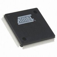
AT91SAM9XE128-QU Atmel, AT91SAM9XE128-QU Datasheet - Page 240

AT91SAM9XE128-QU
Manufacturer Part Number
AT91SAM9XE128-QU
Description
MCU ARM9 128K FLASH 208-PQFP
Manufacturer
Atmel
Series
AT91SAMr
Specifications of AT91SAM9XE128-QU
Core Processor
ARM9
Core Size
16/32-Bit
Speed
180MHz
Connectivity
EBI/EMI, Ethernet, I²C, MMC, SPI, SSC, UART/USART, USB
Peripherals
Brown-out Detect/Reset, POR, PWM, WDT
Number Of I /o
96
Program Memory Size
128KB (128K x 8)
Program Memory Type
FLASH
Ram Size
40K x 8
Voltage - Supply (vcc/vdd)
1.65 V ~ 1.95 V
Data Converters
A/D 4x10b
Oscillator Type
Internal
Operating Temperature
-40°C ~ 85°C
Package / Case
208-MQFP, 208-PQFP
Processor Series
AT91SAMx
Core
ARM926EJ-S
Data Bus Width
32 bit
Data Ram Size
16 KB
Interface Type
2-Wire, EBI, I2S, SPI, USART
Maximum Clock Frequency
180 MHz
Number Of Programmable I/os
96
Number Of Timers
6
Maximum Operating Temperature
+ 85 C
Mounting Style
SMD/SMT
3rd Party Development Tools
JTRACE-ARM-2M, KSK-AT91SAM9XE-PL, MDK-ARM, RL-ARM, ULINK2
Development Tools By Supplier
AT91SAM-ICE, AT91-ISP, AT91SAM9XE-EK
Minimum Operating Temperature
- 40 C
On-chip Adc
10 bit, 4 Channel
For Use With
AT91SAM9XE-EK - KIT EVAL FOR AT91SAM9XEAT91SAM-ICE - EMULATOR FOR AT91 ARM7/ARM9
Lead Free Status / RoHS Status
Lead free / RoHS Compliant
Eeprom Size
-
Lead Free Status / Rohs Status
Lead free / RoHS Compliant
Available stocks
Company
Part Number
Manufacturer
Quantity
Price
- Current page: 240 of 860
- Download datasheet (13Mb)
24.3
24.3.1
24.3.1.1
Table 24-2.
Table 24-3.
Table 24-4.
Notes:
240
27
27
27
Bk[1:0]
26
26
26
Bk[1:0]
Bk[1:0]
Application Example
1. M[1:0] is the byte address inside a 32-bit word.
3. Bk[1] = BA1, Bk[0] = BA0.
AT91SAM9XE128/256/512 Preliminary
25
25
25
Software Interface
Bk[1:0]
Bk[1:0]
Bk[1:0]
32-bit Memory Data Bus Width
24
24
24
SDRAM Configuration Mapping: 2K Rows, 256/512/1024/2048 Columns
SDRAM Configuration Mapping: 4K Rows, 256/512/1024/2048 Columns
SDRAM Configuration Mapping: 8K Rows, 256/512/1024/2048 Columns
Bk[1:0]
Bk[1:0]
Bk[1:0]
23
23
23
Bk[1:0]
Bk[1:0]
22
22
22
Bk[1:0]
The SDRAM address space is organized into banks, rows, and columns. The SDRAM controller
allows mapping different memory types according to the values set in the SDRAMC configura-
tion register.
The SDRAM Controller’s function is to make the SDRAM device access protocol transparent to
the user.
user in correlation with the device structure. Various configurations are illustrated.
21
21
21
20
20
20
Row[12:0]
Row[11:0]
Table 24-2
19
19
19
Row[10:0]
Row[12:0]
Row[11:0]
18
18
18
Row[10:0]
Row[12:0]
Row[11:0]
17
17
17
Row[10:0]
Row[12:0]
to
Row[11:0]
16
16
16
Table 24-7
Row[10:0]
15
15
15
CPU Address Line
CPU Address Line
CPU Address Line
14
14
14
illustrate the SDRAM device memory mapping seen by the
13
13
13
12
12
12
11
11
11
10
10
10
9
9
9
8
8
8
Column[10:0]
Column[10:0]
Column[10:0]
Column[9:0]
Column[9:0]
Column[9:0]
7
7
7
Column[8:0]
Column[8:0]
Column[8:0]
Column[7:0]
Column[7:0]
Column[7:0]
6
6
6
5
5
5
4
4
4
6254C–ATARM–22-Jan-10
3
3
3
2
2
2
1
1
1
M[1:0]
M[1:0]
M[1:0]
M[1:0]
M[1:0]
M[1:0]
M[1:0]
M[1:0]
M[1:0]
M[1:0]
M[1:0]
M[1:0]
0
0
0
Related parts for AT91SAM9XE128-QU
Image
Part Number
Description
Manufacturer
Datasheet
Request
R

Part Number:
Description:
KIT EVAL FOR AT91SAM9XE
Manufacturer:
Atmel
Datasheet:

Part Number:
Description:
MCU ARM9 64K SRAM 144-LFBGA
Manufacturer:
Atmel
Datasheet:

Part Number:
Description:
IC ARM7 MCU FLASH 256K 100LQFP
Manufacturer:
Atmel
Datasheet:

Part Number:
Description:
IC ARM9 MPU 217-LFBGA
Manufacturer:
Atmel
Datasheet:

Part Number:
Description:
MCU ARM9 ULTRA LOW PWR 217-LFBGA
Manufacturer:
Atmel
Datasheet:

Part Number:
Description:
MCU ARM9 324-TFBGA
Manufacturer:
Atmel
Datasheet:

Part Number:
Description:
IC MCU ARM9 SAMPLING 217CBGA
Manufacturer:
Atmel
Datasheet:

Part Number:
Description:
IC ARM9 MCU 217-LFBGA
Manufacturer:
Atmel
Datasheet:

Part Number:
Description:
IC ARM9 MCU 208-PQFP
Manufacturer:
Atmel
Datasheet:

Part Number:
Description:
MCU ARM 512K HS FLASH 100-LQFP
Manufacturer:
Atmel
Datasheet:

Part Number:
Description:
MCU ARM 512K HS FLASH 100-TFBGA
Manufacturer:
Atmel
Datasheet:

Part Number:
Description:
IC ARM9 MCU 200 MHZ 324-TFBGA
Manufacturer:
Atmel
Datasheet:

Part Number:
Description:
IC ARM MCU 16BIT 128K 256BGA
Manufacturer:
Atmel
Datasheet:

Part Number:
Description:
IC ARM7 MCU 32BIT 128K 64LQFP
Manufacturer:
Atmel
Datasheet:

Part Number:
Description:
IC ARM7 MCU FLASH 256K 128-LQFP
Manufacturer:
Atmel
Datasheet:


