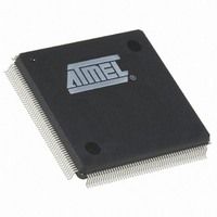
AT91SAM9XE128-QU Atmel, AT91SAM9XE128-QU Datasheet - Page 94

AT91SAM9XE128-QU
Manufacturer Part Number
AT91SAM9XE128-QU
Description
MCU ARM9 128K FLASH 208-PQFP
Manufacturer
Atmel
Series
AT91SAMr
Specifications of AT91SAM9XE128-QU
Core Processor
ARM9
Core Size
16/32-Bit
Speed
180MHz
Connectivity
EBI/EMI, Ethernet, I²C, MMC, SPI, SSC, UART/USART, USB
Peripherals
Brown-out Detect/Reset, POR, PWM, WDT
Number Of I /o
96
Program Memory Size
128KB (128K x 8)
Program Memory Type
FLASH
Ram Size
40K x 8
Voltage - Supply (vcc/vdd)
1.65 V ~ 1.95 V
Data Converters
A/D 4x10b
Oscillator Type
Internal
Operating Temperature
-40°C ~ 85°C
Package / Case
208-MQFP, 208-PQFP
Processor Series
AT91SAMx
Core
ARM926EJ-S
Data Bus Width
32 bit
Data Ram Size
16 KB
Interface Type
2-Wire, EBI, I2S, SPI, USART
Maximum Clock Frequency
180 MHz
Number Of Programmable I/os
96
Number Of Timers
6
Maximum Operating Temperature
+ 85 C
Mounting Style
SMD/SMT
3rd Party Development Tools
JTRACE-ARM-2M, KSK-AT91SAM9XE-PL, MDK-ARM, RL-ARM, ULINK2
Development Tools By Supplier
AT91SAM-ICE, AT91-ISP, AT91SAM9XE-EK
Minimum Operating Temperature
- 40 C
On-chip Adc
10 bit, 4 Channel
For Use With
AT91SAM9XE-EK - KIT EVAL FOR AT91SAM9XEAT91SAM-ICE - EMULATOR FOR AT91 ARM7/ARM9
Lead Free Status / RoHS Status
Lead free / RoHS Compliant
Eeprom Size
-
Lead Free Status / Rohs Status
Lead free / RoHS Compliant
Available stocks
Company
Part Number
Manufacturer
Quantity
Price
- Current page: 94 of 860
- Download datasheet (13Mb)
14.3
14.3.1
Table 14-17. Signal Description List
94
Signal Name
VDDBU
VDDIO
VDDCORE
VDDPLL
GND
XIN
Serial Fast Flash Programming
AT91SAM9XE128/256/512 Preliminary
Device Configuration
Function
Backup Power Supply
I/O Lines Power Supply
Core Power Supply
PLL Power Supply
Ground
Main Clock Input.
This input can be tied to GND. In this
case, the device is clocked by the internal
RC oscillator.
The Serial Fast Flash programming interface is based on IEEE Std. 1149.1 “Standard Test
Access Port and Boundary-Scan Architecture”. Refer to this standard for an explanation of terms
used in this chapter and for a description of the TAP controller states.
In this mode, data read/written from/to the embedded Flash of the device are transmitted
through the JTAG interface of the device.
In Serial Fast Flash Programming Mode, the device is in a specific test mode. Only a distinct set
of pins is significant. Other pins must be left unconnected.
Figure 14-4. Serial Programming
0-50MHz
VDDBU
VDDIO
VDDIO
GND
GND
TDO
TMS
TCK
TDI
Clocks
Power
TST
PGMEN0
PGMEN1
PGMEN2
PGMEN3
XIN
Ground
Power
Power
Power
Power
Type
Input
Active
Level
Comments
32 kHz to 50 MHz
GND
VDDIO
VDDPLL
VDDCORE
6254C–ATARM–22-Jan-10
Related parts for AT91SAM9XE128-QU
Image
Part Number
Description
Manufacturer
Datasheet
Request
R

Part Number:
Description:
KIT EVAL FOR AT91SAM9XE
Manufacturer:
Atmel
Datasheet:

Part Number:
Description:
MCU ARM9 64K SRAM 144-LFBGA
Manufacturer:
Atmel
Datasheet:

Part Number:
Description:
IC ARM7 MCU FLASH 256K 100LQFP
Manufacturer:
Atmel
Datasheet:

Part Number:
Description:
IC ARM9 MPU 217-LFBGA
Manufacturer:
Atmel
Datasheet:

Part Number:
Description:
MCU ARM9 ULTRA LOW PWR 217-LFBGA
Manufacturer:
Atmel
Datasheet:

Part Number:
Description:
MCU ARM9 324-TFBGA
Manufacturer:
Atmel
Datasheet:

Part Number:
Description:
IC MCU ARM9 SAMPLING 217CBGA
Manufacturer:
Atmel
Datasheet:

Part Number:
Description:
IC ARM9 MCU 217-LFBGA
Manufacturer:
Atmel
Datasheet:

Part Number:
Description:
IC ARM9 MCU 208-PQFP
Manufacturer:
Atmel
Datasheet:

Part Number:
Description:
MCU ARM 512K HS FLASH 100-LQFP
Manufacturer:
Atmel
Datasheet:

Part Number:
Description:
MCU ARM 512K HS FLASH 100-TFBGA
Manufacturer:
Atmel
Datasheet:

Part Number:
Description:
IC ARM9 MCU 200 MHZ 324-TFBGA
Manufacturer:
Atmel
Datasheet:

Part Number:
Description:
IC ARM MCU 16BIT 128K 256BGA
Manufacturer:
Atmel
Datasheet:

Part Number:
Description:
IC ARM7 MCU 32BIT 128K 64LQFP
Manufacturer:
Atmel
Datasheet:

Part Number:
Description:
IC ARM7 MCU FLASH 256K 128-LQFP
Manufacturer:
Atmel
Datasheet:


