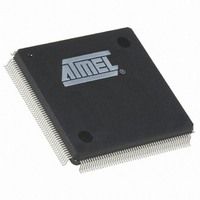
AT91SAM9XE128-QU Atmel, AT91SAM9XE128-QU Datasheet - Page 96

AT91SAM9XE128-QU
Manufacturer Part Number
AT91SAM9XE128-QU
Description
MCU ARM9 128K FLASH 208-PQFP
Manufacturer
Atmel
Series
AT91SAMr
Specifications of AT91SAM9XE128-QU
Core Processor
ARM9
Core Size
16/32-Bit
Speed
180MHz
Connectivity
EBI/EMI, Ethernet, I²C, MMC, SPI, SSC, UART/USART, USB
Peripherals
Brown-out Detect/Reset, POR, PWM, WDT
Number Of I /o
96
Program Memory Size
128KB (128K x 8)
Program Memory Type
FLASH
Ram Size
40K x 8
Voltage - Supply (vcc/vdd)
1.65 V ~ 1.95 V
Data Converters
A/D 4x10b
Oscillator Type
Internal
Operating Temperature
-40°C ~ 85°C
Package / Case
208-MQFP, 208-PQFP
Processor Series
AT91SAMx
Core
ARM926EJ-S
Data Bus Width
32 bit
Data Ram Size
16 KB
Interface Type
2-Wire, EBI, I2S, SPI, USART
Maximum Clock Frequency
180 MHz
Number Of Programmable I/os
96
Number Of Timers
6
Maximum Operating Temperature
+ 85 C
Mounting Style
SMD/SMT
3rd Party Development Tools
JTRACE-ARM-2M, KSK-AT91SAM9XE-PL, MDK-ARM, RL-ARM, ULINK2
Development Tools By Supplier
AT91SAM-ICE, AT91-ISP, AT91SAM9XE-EK
Minimum Operating Temperature
- 40 C
On-chip Adc
10 bit, 4 Channel
For Use With
AT91SAM9XE-EK - KIT EVAL FOR AT91SAM9XEAT91SAM-ICE - EMULATOR FOR AT91 ARM7/ARM9
Lead Free Status / RoHS Status
Lead free / RoHS Compliant
Eeprom Size
-
Lead Free Status / Rohs Status
Lead free / RoHS Compliant
Available stocks
Company
Part Number
Manufacturer
Quantity
Price
- Current page: 96 of 860
- Download datasheet (13Mb)
14.3.3
14.3.4
96
AT91SAM9XE128/256/512 Preliminary
Read/Write Handshake
Device Operations
The read/write handshake is done by carrying out read/write operations on two registers of the
device that are accessible through the JTAG:
Access to these registers is done through the TAP 38-bit DR register comprising a 32-bit data
field, a 5-bit address field and a read/write bit. The data to be written is scanned into the 32-bit
data field with the address of the register to the 5-bit address field and 1 to the read/write bit. A
register is read by scanning its address into the address field and 0 into the read/write bit, going
through the UPDATE-DR TAP state, then scanning out the data.
Refer to the ARM7TDMI reference manuel for more information on Comm channel operations.
Figure 14-5. TAP 8-bit DR Register
A read or write takes place when the TAP controller enters UPDATE-DR state. Refer to the IEEE
1149.1 for more details on JTAG operations.
The write handshake is done by polling the Debug Comms Control Register until the R bit is
cleared. Once cleared, data can be written to the Debug Comms Data Register.
The read handshake is done by polling the Debug Comms Control Register until the W bit is set.
Once set, data can be read in the Debug Comms Data Register.
Several commands on the Flash memory are available. These commands are summarized in
Table 14-3 on page
is reading and writing the Debug Comms Registers.
TDI
• Debug Comms Control Register: DCCR
• Debug Comms Data Register: DCDR
• The address of the Debug Comms Control Register is 0x04.
• The address of the Debug Comms Data Register is 0x05.
The Debug Comms Control Register is read-only and allows synchronized handshaking
between the processor and the debugger.
– Bit 1 (W): Denotes whether the programmer can read a data through the Debug
– Bit 0 (R): Denotes whether the programmer can send data from the Debug Comms
Comms Data Register. If the device is busy W = 0, then the programmer must poll
until W = 1.
Data Register. If R = 1, data previously placed there through the scan chain has not
been collected by the device and so the programmer must wait.
r/w
4
Address
Address
Decoder
87. Commands are run by the programmer through the serial interface that
5
0
31
Debug Comms Control Register
Debug Comms Data Register
Data
32
6254C–ATARM–22-Jan-10
0
TDO
Related parts for AT91SAM9XE128-QU
Image
Part Number
Description
Manufacturer
Datasheet
Request
R

Part Number:
Description:
KIT EVAL FOR AT91SAM9XE
Manufacturer:
Atmel
Datasheet:

Part Number:
Description:
MCU ARM9 64K SRAM 144-LFBGA
Manufacturer:
Atmel
Datasheet:

Part Number:
Description:
IC ARM7 MCU FLASH 256K 100LQFP
Manufacturer:
Atmel
Datasheet:

Part Number:
Description:
IC ARM9 MPU 217-LFBGA
Manufacturer:
Atmel
Datasheet:

Part Number:
Description:
MCU ARM9 ULTRA LOW PWR 217-LFBGA
Manufacturer:
Atmel
Datasheet:

Part Number:
Description:
MCU ARM9 324-TFBGA
Manufacturer:
Atmel
Datasheet:

Part Number:
Description:
IC MCU ARM9 SAMPLING 217CBGA
Manufacturer:
Atmel
Datasheet:

Part Number:
Description:
IC ARM9 MCU 217-LFBGA
Manufacturer:
Atmel
Datasheet:

Part Number:
Description:
IC ARM9 MCU 208-PQFP
Manufacturer:
Atmel
Datasheet:

Part Number:
Description:
MCU ARM 512K HS FLASH 100-LQFP
Manufacturer:
Atmel
Datasheet:

Part Number:
Description:
MCU ARM 512K HS FLASH 100-TFBGA
Manufacturer:
Atmel
Datasheet:

Part Number:
Description:
IC ARM9 MCU 200 MHZ 324-TFBGA
Manufacturer:
Atmel
Datasheet:

Part Number:
Description:
IC ARM MCU 16BIT 128K 256BGA
Manufacturer:
Atmel
Datasheet:

Part Number:
Description:
IC ARM7 MCU 32BIT 128K 64LQFP
Manufacturer:
Atmel
Datasheet:

Part Number:
Description:
IC ARM7 MCU FLASH 256K 128-LQFP
Manufacturer:
Atmel
Datasheet:


