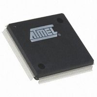
AT91SAM9XE128-QU Atmel, AT91SAM9XE128-QU Datasheet - Page 756

AT91SAM9XE128-QU
Manufacturer Part Number
AT91SAM9XE128-QU
Description
MCU ARM9 128K FLASH 208-PQFP
Manufacturer
Atmel
Series
AT91SAMr
Specifications of AT91SAM9XE128-QU
Core Processor
ARM9
Core Size
16/32-Bit
Speed
180MHz
Connectivity
EBI/EMI, Ethernet, I²C, MMC, SPI, SSC, UART/USART, USB
Peripherals
Brown-out Detect/Reset, POR, PWM, WDT
Number Of I /o
96
Program Memory Size
128KB (128K x 8)
Program Memory Type
FLASH
Ram Size
40K x 8
Voltage - Supply (vcc/vdd)
1.65 V ~ 1.95 V
Data Converters
A/D 4x10b
Oscillator Type
Internal
Operating Temperature
-40°C ~ 85°C
Package / Case
208-MQFP, 208-PQFP
Processor Series
AT91SAMx
Core
ARM926EJ-S
Data Bus Width
32 bit
Data Ram Size
16 KB
Interface Type
2-Wire, EBI, I2S, SPI, USART
Maximum Clock Frequency
180 MHz
Number Of Programmable I/os
96
Number Of Timers
6
Maximum Operating Temperature
+ 85 C
Mounting Style
SMD/SMT
3rd Party Development Tools
JTRACE-ARM-2M, KSK-AT91SAM9XE-PL, MDK-ARM, RL-ARM, ULINK2
Development Tools By Supplier
AT91SAM-ICE, AT91-ISP, AT91SAM9XE-EK
Minimum Operating Temperature
- 40 C
On-chip Adc
10 bit, 4 Channel
For Use With
AT91SAM9XE-EK - KIT EVAL FOR AT91SAM9XEAT91SAM-ICE - EMULATOR FOR AT91 ARM7/ARM9
Lead Free Status / RoHS Status
Lead free / RoHS Compliant
Eeprom Size
-
Lead Free Status / Rohs Status
Lead free / RoHS Compliant
Available stocks
Company
Part Number
Manufacturer
Quantity
Price
- Current page: 756 of 860
- Download datasheet (13Mb)
41.3.4.3
41.3.4.4
41.3.4.5
756
AT91SAM9XE128/256/512 Preliminary
Memory Interface
FIFO and DMA Features
Example
Preview datapath contains a data formatter that converts 8:8:8 pixel to RGB 5:5:5 format compli-
ant with 16-bit format of the LCD controller. In general, when converting from a color channel
with more bits to one with fewer bits, formatter module discards the lower-order bits. Example:
Converting from RGB 8:8:8 to RGB 5:6:5, it discards the three LSBs from the red and blue chan-
nels, and two LSBs from the green channel. When grayscale mode is enabled, two memory
format are supported. One mode supports 2 pixels per word, and the other mode supports 1
pixel per word.
Table 41-8.
Both preview and Codec datapaths contain FIFOs, asynchronous buffers that are used to safely
transfer formatted pixels from Pixel clock domain to AHB clock domain. A video arbiter is used to
manage FIFO thresholds and triggers a relevant DMA request through the AHB master inter-
face. Thus, depending on FIFO state, a specified length burst is asserted. Regarding AHB
master interface, it supports Scatter DMA mode through linked list operation. This mode of oper-
ation improves flexibility of image buffer location and allows the user to allocate two or more
frame buffers. The destination frame buffers are defined by a series of Frame Buffer Descriptors
(FBD). Each FBD controls the transfer of one entire frame and then optionally loads a further
FBD to switch the DMA operation at another frame buffer address. The FBD is defined by a
series of two words. The first one defines the current frame buffer address, and the second
defines the next FBD memory location. This DMA transfer mode is only available for preview
datapath and is configured in the ISI_PPFBD register that indicates the memory location of the
first FBD.
The primary FBD is programmed into the camera interface controller. The data to be transferred
described by an FBD requires several burst access. In the example below, the use of 2 ping-
pong frame buffers is described.
The first FBD, stored at address 0x30000, defines the location of the first frame buffer.
Destination Address: frame buffer ID0 0x02A000
Next FBD address: 0x30010
Second FBD, stored at address 0x30010, defines the location of the second frame buffer.
Destination Address: frame buffer ID1 0x3A000
Transfer width: 32 bit
Next FBD address: 0x30000, wrapping to first FBD.
Using this technique, several frame buffers can be configured through the linked list.
illustrates a typical three frame buffer application. Frame n is mapped to frame buffer 0, frame
n+1 is mapped to frame buffer 1, frame n+2 is mapped to Frame buffer 2, further frames wrap. A
codec request occurs, and the full-size 4:2:2 encoded frame is stored in a dedicated memory
space.
GS_MODE
0
1
Grayscale Memory Mapping Configuration for 12-bit Data
P_0[11:4]
P_0[11:4]
DATA[31:24]
DATA[23:16]
P_0[3:0], 0000
P_0[3:0], 0000
DATA[15:8]
P_1[11:4]
0
DATA[7:0]
P_1[3:0], 0000
0
6254C–ATARM–22-Jan-10
Figure 41-6
Related parts for AT91SAM9XE128-QU
Image
Part Number
Description
Manufacturer
Datasheet
Request
R

Part Number:
Description:
KIT EVAL FOR AT91SAM9XE
Manufacturer:
Atmel
Datasheet:

Part Number:
Description:
MCU ARM9 64K SRAM 144-LFBGA
Manufacturer:
Atmel
Datasheet:

Part Number:
Description:
IC ARM7 MCU FLASH 256K 100LQFP
Manufacturer:
Atmel
Datasheet:

Part Number:
Description:
IC ARM9 MPU 217-LFBGA
Manufacturer:
Atmel
Datasheet:

Part Number:
Description:
MCU ARM9 ULTRA LOW PWR 217-LFBGA
Manufacturer:
Atmel
Datasheet:

Part Number:
Description:
MCU ARM9 324-TFBGA
Manufacturer:
Atmel
Datasheet:

Part Number:
Description:
IC MCU ARM9 SAMPLING 217CBGA
Manufacturer:
Atmel
Datasheet:

Part Number:
Description:
IC ARM9 MCU 217-LFBGA
Manufacturer:
Atmel
Datasheet:

Part Number:
Description:
IC ARM9 MCU 208-PQFP
Manufacturer:
Atmel
Datasheet:

Part Number:
Description:
MCU ARM 512K HS FLASH 100-LQFP
Manufacturer:
Atmel
Datasheet:

Part Number:
Description:
MCU ARM 512K HS FLASH 100-TFBGA
Manufacturer:
Atmel
Datasheet:

Part Number:
Description:
IC ARM9 MCU 200 MHZ 324-TFBGA
Manufacturer:
Atmel
Datasheet:

Part Number:
Description:
IC ARM MCU 16BIT 128K 256BGA
Manufacturer:
Atmel
Datasheet:

Part Number:
Description:
IC ARM7 MCU 32BIT 128K 64LQFP
Manufacturer:
Atmel
Datasheet:

Part Number:
Description:
IC ARM7 MCU FLASH 256K 128-LQFP
Manufacturer:
Atmel
Datasheet:


