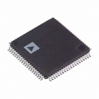
ADUC7129BSTZ126-RL Analog Devices Inc, ADUC7129BSTZ126-RL Datasheet - Page 24

ADUC7129BSTZ126-RL
Manufacturer Part Number
ADUC7129BSTZ126-RL
Description
IC DAS MCU ARM7 ADC/DDS 80-LQFP
Manufacturer
Analog Devices Inc
Series
MicroConverter® ADuC7xxxr
Datasheet
1.EVAL-ADUC7128QSPZ.pdf
(92 pages)
Specifications of ADUC7129BSTZ126-RL
Core Size
16/32-Bit
Program Memory Size
126KB (126K x 8)
Core Processor
ARM7
Speed
41.78MHz
Connectivity
EBI/EMI, I²C, SPI, UART/USART
Peripherals
PLA, POR, PWM, PSM, Temp Sensor, WDT
Number Of I /o
38
Program Memory Type
FLASH
Ram Size
8K x 8
Voltage - Supply (vcc/vdd)
3 V ~ 3.6 V
Data Converters
A/D 10x12b; D/A 1x10b
Oscillator Type
Internal
Operating Temperature
-40°C ~ 125°C
Package / Case
80-LQFP
Controller Family/series
(ARM7) ADUC
No. Of I/o's
40
Cpu Speed
41.78MHz
No. Of Timers
5
Digital Ic Case Style
LQFP
Embedded Interface Type
I2C, SPI, UART
Rohs Compliant
Yes
Lead Free Status / RoHS Status
Lead free / RoHS Compliant
Eeprom Size
-
Lead Free Status / RoHS Status
Lead free / RoHS Compliant, Lead free / RoHS Compliant
Other names
ADUC7129BSTZ126-RLTR
Available stocks
Company
Part Number
Manufacturer
Quantity
Price
Company:
Part Number:
ADUC7129BSTZ126-RL
Manufacturer:
Analog Devices Inc
Quantity:
10 000
ADuC7128/ADuC7129
TERMINOLOGY
ADC SPECIFICATIONS
Integral Nonlinearity
The maximum deviation of any code from a straight line
passing through the endpoints of the ADC transfer function.
The endpoints of the transfer function are zero scale, a point
½ LSB below the first code transition and full scale, a point
½ LSB above the last code transition.
Differential Nonlinearity
The difference between the measured and the ideal 1 LSB
change between any two adjacent codes in the ADC.
Offset Error
The deviation of the first code transition (0000 . . . 000) to
(0000 . . . 001) from the ideal, that is, +½ LSB.
Gain Error
The deviation of the last code transition from the ideal AIN
voltage (full scale − 1.5 LSB) after the offset error has been
adjusted out.
Signal to (Noise + Distortion) Ratio
The measured ratio of signal to (noise + distortion) at the
output of the ADC. The signal is the rms amplitude of the
fundamental. Noise is the rms sum of all nonfundamental
signals up to half the sampling frequency (f
dc. The ratio is dependent on the number of quantization
levels in the digitization process; the more levels, the smaller
the quantization noise.
S
/2), excluding
Rev. 0 | Page 24 of 92
The theoretical signal to (noise + distortion) ratio for an ideal
N-bit converter with a sine wave input is given by
Thus, for a 12-bit converter, this is 74 dB.
Total Harmonic Distortion
The ratio of the rms sum of the harmonics to the fundamental.
DAC SPECIFICATIONS
Relative Accuracy
Otherwise known as endpoint linearity, relative accuracy is
a measure of the maximum deviation from a straight line passing
through the endpoints of the DAC transfer function. It is measured
after adjusting for zero error and full-scale error.
Voltage Output Settling Time
The amount of time it takes for the output to settle to within a
1 LSB level for a full-scale input change.
Signal to (Noise + Distortion) = (6.02 N + 1.76) dB


