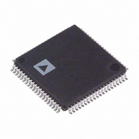
ADUC7129BSTZ126-RL Analog Devices Inc, ADUC7129BSTZ126-RL Datasheet - Page 43

ADUC7129BSTZ126-RL
Manufacturer Part Number
ADUC7129BSTZ126-RL
Description
IC DAS MCU ARM7 ADC/DDS 80-LQFP
Manufacturer
Analog Devices Inc
Series
MicroConverter® ADuC7xxxr
Datasheet
1.EVAL-ADUC7128QSPZ.pdf
(92 pages)
Specifications of ADUC7129BSTZ126-RL
Core Size
16/32-Bit
Program Memory Size
126KB (126K x 8)
Core Processor
ARM7
Speed
41.78MHz
Connectivity
EBI/EMI, I²C, SPI, UART/USART
Peripherals
PLA, POR, PWM, PSM, Temp Sensor, WDT
Number Of I /o
38
Program Memory Type
FLASH
Ram Size
8K x 8
Voltage - Supply (vcc/vdd)
3 V ~ 3.6 V
Data Converters
A/D 10x12b; D/A 1x10b
Oscillator Type
Internal
Operating Temperature
-40°C ~ 125°C
Package / Case
80-LQFP
Controller Family/series
(ARM7) ADUC
No. Of I/o's
40
Cpu Speed
41.78MHz
No. Of Timers
5
Digital Ic Case Style
LQFP
Embedded Interface Type
I2C, SPI, UART
Rohs Compliant
Yes
Lead Free Status / RoHS Status
Lead free / RoHS Compliant
Eeprom Size
-
Lead Free Status / RoHS Status
Lead free / RoHS Compliant, Lead free / RoHS Compliant
Other names
ADUC7129BSTZ126-RLTR
Available stocks
Company
Part Number
Manufacturer
Quantity
Price
Company:
Part Number:
ADUC7129BSTZ126-RL
Manufacturer:
Analog Devices Inc
Quantity:
10 000
Table 44. FEE0PRO and FEE0HID MMR Bit Designations
Bit
31
30:0
Table 45. FEE1PRO and FEE1HID MMR Bit Designations
Bit
31
30
31:0
EXECUTION TIME FROM SRAM AND FLASH/EE
This section describes SRAM and Flash/EE access times during
execution for applications where execution time is critical.
Execution from SRAM
Fetching instructions from SRAM takes one clock cycle because
the access time of the SRAM is 2 ns and a clock cycle is 22 ns
minimum. However, if the instruction involves reading or
writing data to memory, one extra cycle must be added if the
data is in SRAM (or three cycles if the data is in Flash/EE), one
cycle to execute the instruction and two cycles to get the 32-bit
data from Flash/EE. A control flow instruction, such as a branch
instruction, takes one cycle to fetch, but it also takes two cycles
to fill the pipeline with the new instructions.
Execution from Flash/EE
Because the Flash/EE width is 16 bits and access time for 16-bit
words is 23 ns, execution from Flash/EE cannot be done in one
cycle (as can be done from SRAM when the CD bit = 0). In addi-
tion, some dead times are needed before accessing data for any
value of CD bits.
In ARM mode, where instructions are 32 bits, two cycles are
needed to fetch any instruction when CD = 0. In Thumb mode,
where instructions are 16 bits, one cycle is needed to fetch any
instruction.
Description
Read Protection.
Write Protection for Page 123 to Page 120, for Page 119 to Page 116, and for Page 3 to Page 0.
Description
Read Protection.
Write Protection for Page 127 to Page 120.
Write Protection for Page 119 to Page 116 and for Page 3 to Page 0.
Cleared by user to protect Block 0.
Set by user to allow reading Block 0.
Cleared by user to protect the pages in writing.
Set by user to allow writing the pages.
Cleared by user to protect Block 1.
Set by user to allow reading Block 1.
Cleared by user to protect the pages in writing.
Set by user to allow writing the pages.
Cleared by user to protect the pages in writing.
Set by user to allow writing the pages.
Rev. 0 | Page 43 of 92
Timing is identical in both modes when executing instructions
that involve using the Flash/EE for data memory. If the instruction
to be executed is a control flow instruction, an extra cycle is
needed to decode the new address of the program counter and
then four cycles are needed to fill the pipeline. A data processing
instruction involving only core registers doesn’t require any
extra clock cycles, but if it involves data in Flash/EE, an extra
clock cycle is needed to decode the address of the data and two
cycles to get the 32-bit data from Flash/EE. An extra cycle must
also be added before fetching another instruction. Data transfer
instructions are more complex and are summarized in Table 46.
Table 46. Execution Cycles in ARM/Thumb Mode
Instructions
LD
LDH
LDM/PUSH
STR
STRH
STRM/POP
With 1 < N ≤ 16, N is the number of bytes of data to load or
store in the multiple load/store instruction. The SWAP instruction
combines an LD and STR instruction with only one fetch,
giving a total of eight cycles plus 40 μs.
Fetch
Cycles
2/1
2/1
2/1
2/1
2/1
2/1
Dead
Time
1
1
N
1
1
N
ADuC7128/ADuC7129
Data Access
2
1
2 × N
2 × 20 μs
20 μs
2 × N × 20 μs
Dead
Time
1
1
N
1
1
N


