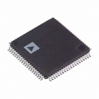
ADUC7129BSTZ126-RL Analog Devices Inc, ADUC7129BSTZ126-RL Datasheet - Page 66

ADUC7129BSTZ126-RL
Manufacturer Part Number
ADUC7129BSTZ126-RL
Description
IC DAS MCU ARM7 ADC/DDS 80-LQFP
Manufacturer
Analog Devices Inc
Series
MicroConverter® ADuC7xxxr
Datasheet
1.EVAL-ADUC7128QSPZ.pdf
(92 pages)
Specifications of ADUC7129BSTZ126-RL
Core Size
16/32-Bit
Program Memory Size
126KB (126K x 8)
Core Processor
ARM7
Speed
41.78MHz
Connectivity
EBI/EMI, I²C, SPI, UART/USART
Peripherals
PLA, POR, PWM, PSM, Temp Sensor, WDT
Number Of I /o
38
Program Memory Type
FLASH
Ram Size
8K x 8
Voltage - Supply (vcc/vdd)
3 V ~ 3.6 V
Data Converters
A/D 10x12b; D/A 1x10b
Oscillator Type
Internal
Operating Temperature
-40°C ~ 125°C
Package / Case
80-LQFP
Controller Family/series
(ARM7) ADUC
No. Of I/o's
40
Cpu Speed
41.78MHz
No. Of Timers
5
Digital Ic Case Style
LQFP
Embedded Interface Type
I2C, SPI, UART
Rohs Compliant
Yes
Lead Free Status / RoHS Status
Lead free / RoHS Compliant
Eeprom Size
-
Lead Free Status / RoHS Status
Lead free / RoHS Compliant, Lead free / RoHS Compliant
Other names
ADUC7129BSTZ126-RLTR
Available stocks
Company
Part Number
Manufacturer
Quantity
Price
Company:
Part Number:
ADUC7129BSTZ126-RL
Manufacturer:
Analog Devices Inc
Quantity:
10 000
ADuC7128/ADuC7129
I2CxSSTA Register
Name
I2C0SSTA
I2C1SSTA
I2CxSSTA is a status register for the slave channel.
Table 93. I2CxSSTA MMR Bit Designations
Bit
31:15
14
13
12:11
10
9:8
7
6
5
4
3
2
1
0
Address
0xFFFF0804
0xFFFF0904
Value
00
01
10
11
00
01
10
11
Description
Reserved. These bits should be written as 0.
START Decode Bit.
Repeated START Decode Bit.
ID Decode Bits.
Received Address Matched ID Register 0.
Received Address Matched ID Register 1.
Received Address Matched ID Register 2.
Received Address Matched ID Register 3.
Stop After Start And Matching Address Interrupt.
General Call ID.
No General Call.
General Call Reset and Program Address.
General Call Program Address.
General Call Matching Alternative ID.
General Call Interrupt.
Slave Busy.
No Acknowledge.
Slave Receive FIFO Overflow.
Slave Receive IRQ.
Slave Transmit IRQ.
Slave Transmit FIFO Underflow.
Slave Transmit FIFO Empty.
Default Value
0x01
0x01
Set by hardware if the device receives a valid start and matching address.
Cleared by an I
Set by hardware if the device receives a valid repeated start and matching address.
Cleared by an I
Set by hardware if the slave device receives an I
and matching address.
Cleared by a read of the I2CxSSTA register.
Set if the slave device receives a general call of any type.
Cleared by setting Bit 8 of the I2CxCFG register. If it is a general call reset, all registers are at their default
values. If it is a hardware general call, the Rx FIFO holds the second byte of the general call. This is similar
to the I2C0ALT register (unless it is a general call to reprogram the device address). For more details, see
the I
Set automatically if the slave is busy.
Cleared automatically.
Set if master asks for data and no data is available.
Cleared automatically by reading the I2C0SSTA register.
Set automatically if the slave receive FIFO is overflowing.
Cleared automatically by reading I2C0SRX register.
Set after receiving data.
Cleared automatically by reading the I2C0SRX register or flushing the FIFO.
Set at the end of a transmission.
Cleared automatically by writing to the I2C0STX register.
Set automatically if the slave transmit FIFO is underflowing.
Cleared automatically by writing to the I2C0STX register.
Set automatically if the slave transmit FIFO is empty.
Cleared automatically by writing twice to the I2C0STX register.
2
C Bus Specification, Version 2.1, Jan. 2000.
2
2
C stop condition or an I
C stop condition, a read of the I2CxSSTA register, or an I
Access
R
R
Rev. 0 | Page 66 of 92
2
C general call reset.
2
C STOP condition after a previous I
2
C general call reset.
2
C START condition


