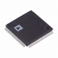
ADUC7129BSTZ126-RL Analog Devices Inc, ADUC7129BSTZ126-RL Datasheet - Page 84

ADUC7129BSTZ126-RL
Manufacturer Part Number
ADUC7129BSTZ126-RL
Description
IC DAS MCU ARM7 ADC/DDS 80-LQFP
Manufacturer
Analog Devices Inc
Series
MicroConverter® ADuC7xxxr
Datasheet
1.EVAL-ADUC7128QSPZ.pdf
(92 pages)
Specifications of ADUC7129BSTZ126-RL
Core Size
16/32-Bit
Program Memory Size
126KB (126K x 8)
Core Processor
ARM7
Speed
41.78MHz
Connectivity
EBI/EMI, I²C, SPI, UART/USART
Peripherals
PLA, POR, PWM, PSM, Temp Sensor, WDT
Number Of I /o
38
Program Memory Type
FLASH
Ram Size
8K x 8
Voltage - Supply (vcc/vdd)
3 V ~ 3.6 V
Data Converters
A/D 10x12b; D/A 1x10b
Oscillator Type
Internal
Operating Temperature
-40°C ~ 125°C
Package / Case
80-LQFP
Controller Family/series
(ARM7) ADUC
No. Of I/o's
40
Cpu Speed
41.78MHz
No. Of Timers
5
Digital Ic Case Style
LQFP
Embedded Interface Type
I2C, SPI, UART
Rohs Compliant
Yes
Lead Free Status / RoHS Status
Lead free / RoHS Compliant
Eeprom Size
-
Lead Free Status / RoHS Status
Lead free / RoHS Compliant, Lead free / RoHS Compliant
Other names
ADUC7129BSTZ126-RLTR
Available stocks
Company
Part Number
Manufacturer
Quantity
Price
Company:
Part Number:
ADUC7129BSTZ126-RL
Manufacturer:
Analog Devices Inc
Quantity:
10 000
ADuC7128/ADuC7129
The XMxPAR are registers that define the protocol used for accessing the external memory for each memory region.
Table 121. XMxPAR MMR Bit Designations
Bit
15
14:12
11
10
9
8
7:4
3:0
TIMING DIAGRAMS
Figure 62 through Figure 65 show the timing for a read cycle (see Figure 62), a read cycle with address hold and bus turn cycles (see
Figure 63), a write cycle with address hold and write hold cycles (see Figure 64), and a write cycle with wait states (see Figure 65).
Description
Enable Byte Write Strobe. This bit is only used for two,
8-bit memory sharing the same memory region.
Number of Wait States on the Address Latch Enable Strobe.
Reserved.
Extra Address Hold Time.
Extra Bus Transition Time on Read.
Extra Bus Transition Time on Write.
Number of Write Wait States. Select the number of wait states added to the length of the WS pulse. 0x0 is 1 clock cycle; 0xF is 16 clock
cycles (default value).
Number of Read Wait States. Select the number of wait states added to the length of the RS pulse. 0x0 is 1 clock cycle; 0xF is 16 clock
cycles (default value).
Set by user to gate the AD0 output with the WS output. This allows byte write capability without using BHE and BLE signals.
Set by the user to disable extra bus transition time.
Cleared by the user to enable one extra clock before and after the read select (RS).
Set by the user to disable extra bus transition time.
Cleared by the user to enable one extra clock before and after the write select (WS).
Cleared by user to use BHE and BLE signals.
Set by the user to disable extra hold time.
Cleared by the user to enable one clock cycle of hold on the address in read and write.
AD16:0
HCLK
MSx
AE
RS
ADDRESS
Figure 62. External Memory Read Cycle
Rev. 0 | Page 84 of 92
DATA


