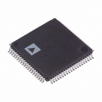
ADUC7129BSTZ126-RL Analog Devices Inc, ADUC7129BSTZ126-RL Datasheet - Page 65

ADUC7129BSTZ126-RL
Manufacturer Part Number
ADUC7129BSTZ126-RL
Description
IC DAS MCU ARM7 ADC/DDS 80-LQFP
Manufacturer
Analog Devices Inc
Series
MicroConverter® ADuC7xxxr
Datasheet
1.EVAL-ADUC7128QSPZ.pdf
(92 pages)
Specifications of ADUC7129BSTZ126-RL
Core Size
16/32-Bit
Program Memory Size
126KB (126K x 8)
Core Processor
ARM7
Speed
41.78MHz
Connectivity
EBI/EMI, I²C, SPI, UART/USART
Peripherals
PLA, POR, PWM, PSM, Temp Sensor, WDT
Number Of I /o
38
Program Memory Type
FLASH
Ram Size
8K x 8
Voltage - Supply (vcc/vdd)
3 V ~ 3.6 V
Data Converters
A/D 10x12b; D/A 1x10b
Oscillator Type
Internal
Operating Temperature
-40°C ~ 125°C
Package / Case
80-LQFP
Controller Family/series
(ARM7) ADUC
No. Of I/o's
40
Cpu Speed
41.78MHz
No. Of Timers
5
Digital Ic Case Style
LQFP
Embedded Interface Type
I2C, SPI, UART
Rohs Compliant
Yes
Lead Free Status / RoHS Status
Lead free / RoHS Compliant
Eeprom Size
-
Lead Free Status / RoHS Status
Lead free / RoHS Compliant, Lead free / RoHS Compliant
Other names
ADUC7129BSTZ126-RLTR
Available stocks
Company
Part Number
Manufacturer
Quantity
Price
Company:
Part Number:
ADUC7129BSTZ126-RL
Manufacturer:
Analog Devices Inc
Quantity:
10 000
I
The ADuC7128/ADuC7129 support two fully licensed I
interfaces. The I
hardware master and slave interfaces. Because the two I
interfaces are identical, only I
that the two masters and slaves have individual interrupts.
Note that when configured as an I
ADuC7128/ADuC7129 cannot generate a repeated start
condition.
The two pins used for data transfer, SDA and SCL, are configured
in a wire-AND’ e d format that allows arbitration in a multimaster
system. These pins require external pull-up resistors. Typical
pull-up values are 10 kΩ.
The I
programmed by the user. This ID can be modified any time a
transfer is not in progress. The user can configure the interface
to respond to four slave addresses.
The transfer sequence of an I
device initiating a transfer by generating a start condition while
the bus is idle. The master transmits the address of the slave
device and the direction of the data transfer in the initial
address transfer. If the master does not lose arbitration and the
slave acknowledges, then the data transfer is initiated. This
continues until the master issues a stop condition and the bus
becomes idle.
The I
independent and can be simultaneously active. A slave is
activated when a transfer has been initiated on the bus.
If it is not addressed, it remains inactive until another transfer is
initiated. This also allows a master device, which has lost
arbitration, to respond as a slave in the same cycle.
Serial Clock Generation
The I
transfer. The master channel can be configured to operate in
fast mode (400 kHz) or standard mode (100 kHz).
The bit rate is defined in the I2C0DIV MMR as follows:
where:
f
DIVH is the high period of the clock.
DIVL is the low period of the clock.
Thus, for 100 kHz operation
and for 400 kHz
The I2CxDIV register corresponds to DIVH:DIVL.
UCLK
2
C-COMPATIBLE INTERFACES
DIVH = DIVL = 0xCF
DIVH = 0x28 DIVL = 0x3C.
is the clock before the clock divider.
2
2
2
f
C bus peripheral addresses in the I
C peripheral master and slave functionality are
C master in the system generates the serial clock for a
S
ERIAL
CLOCK
2
=
C interfaces are both implemented as full
2 (
+
DIVH
f
UCLK
)
2
+
2
C system consists of a master
C0 is described in detail. Note
(2
+
2
C master device, the
DIVL
)
2
C bus system are
2
2
C
C
Rev. 0 | Page 65 of 92
Slave Addresses
Register I2C0ID0, Register I2C0ID1, Register I2C0ID2, and
Register I2C0ID3 contain the device IDs. The device compares
the four I2C0IDx registers to the address byte. The seven most
significant bits of either ID register must be identical to that of
the seven most significant bits of the first address byte received
to be correctly addressed. The LSB of the ID registers, transfer
direction bit, is ignored in the process of address recognition.
I
The I
discussed in this section.
I2CxMSTA Register
Name
I2C0MSTA
I2C1MSTA
I2CxMSTA is a status register for the master channel.
Table 92. I2C0MSTA MMR Bit Designations
Bit
7
6
5
4
3
2
1
0
2
C REGISTERS
2
Description
Master Transmit FIFO Flush.
Master Busy.
Arbitration Loss.
No Acknowledge.
Master Receive IRQ.
Master Transmit IRQ.
Master Transmit FIFO Underflow.
Master TX FIFO Not Full.
C peripheral interface consists of 18 MMRs that are
Set by user to flush the master Tx FIFO.
Cleared automatically once the master Tx FIFO is flushed.
This bit also flushes the slave receive FIFO.
Set automatically if the master is busy.
Cleared automatically.
Set in multimaster mode if another master has the bus.
Cleared when the bus becomes available.
Set automatically if there is no acknowledge of the
address by the slave device.
Cleared automatically by reading the I2C0MSTA register.
Set after receiving data.
Cleared automatically by reading the I2C0MRX register.
Set at the end of a transmission.
Cleared automatically by writing to the I2C0MTX register.
Set automatically if the master transmit FIFO is
underflowing.
Cleared automatically by writing to the I2C0MTX register.
Set automatically if the slave transmit FIFO is not full.
Cleared automatically by writing twice to the I2C0STX
register.
Address
0xFFFF0800
0xFFFF0900
ADuC7128/ADuC7129
Default Value
0x00
0x00
Access
R
R


