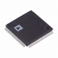
ADUC7129BSTZ126-RL Analog Devices Inc, ADUC7129BSTZ126-RL Datasheet - Page 4

ADUC7129BSTZ126-RL
Manufacturer Part Number
ADUC7129BSTZ126-RL
Description
IC DAS MCU ARM7 ADC/DDS 80-LQFP
Manufacturer
Analog Devices Inc
Series
MicroConverter® ADuC7xxxr
Datasheet
1.EVAL-ADUC7128QSPZ.pdf
(92 pages)
Specifications of ADUC7129BSTZ126-RL
Core Size
16/32-Bit
Program Memory Size
126KB (126K x 8)
Core Processor
ARM7
Speed
41.78MHz
Connectivity
EBI/EMI, I²C, SPI, UART/USART
Peripherals
PLA, POR, PWM, PSM, Temp Sensor, WDT
Number Of I /o
38
Program Memory Type
FLASH
Ram Size
8K x 8
Voltage - Supply (vcc/vdd)
3 V ~ 3.6 V
Data Converters
A/D 10x12b; D/A 1x10b
Oscillator Type
Internal
Operating Temperature
-40°C ~ 125°C
Package / Case
80-LQFP
Controller Family/series
(ARM7) ADUC
No. Of I/o's
40
Cpu Speed
41.78MHz
No. Of Timers
5
Digital Ic Case Style
LQFP
Embedded Interface Type
I2C, SPI, UART
Rohs Compliant
Yes
Lead Free Status / RoHS Status
Lead free / RoHS Compliant
Eeprom Size
-
Lead Free Status / RoHS Status
Lead free / RoHS Compliant, Lead free / RoHS Compliant
Other names
ADUC7129BSTZ126-RLTR
Available stocks
Company
Part Number
Manufacturer
Quantity
Price
Company:
Part Number:
ADUC7129BSTZ126-RL
Manufacturer:
Analog Devices Inc
Quantity:
10 000
ADuC7128/ADuC7129
SPECIFICATIONS
AV
otherwise noted.
Table 1.
Parameter
ADC CHANNEL SPECIFICATIONS
ENDPOINT ERRORS
DYNAMIC PERFORMANCE
ANALOG INPUT
ON-CHIP VOLTAGE REFERENCE
EXTERNAL REFERENCE INPUT
DAC CHANNEL SPECIFICATIONS
Offset Error
Offset Error Match
Output Voltage
Input Impedance
ADC Power-Up Time
DC Accuracy
Gain Error
Gain Error Match
Signal-to-Noise Ratio (SNR)
Total Harmonic Distortion (THD)
Peak Harmonic or Spurious Noise
Channel-to-Channel Crosstalk
Crosstalk Between Channel 12 and
Input Voltage Ranges
Leakage Current
Input Capacitance
Accuracy
Reference Drop When DAC Enabled
Reference Temperature Coefficient
Power Supply Rejection Ratio
Output Impedance
Internal V
Input Voltage Range
VDAC Output
DD
Differential Mode
Single-Ended Mode
Resolution
Integral Nonlinearity
Differential Nonlinearity
DC Code Distribution
Channel 13
Voltage Swing
I/V Output Resistance
Low-Pass Filter 3 dB Point
Resolution
= IOV
REF
DD
Power-On Time
1, 2
= 3.0 V to 3.6 V, V
4
5
3
3
6
REF
= 2.5 V internal reference, f
Min
12
0.625
Typ
5
±0.7
±0.7
±2.0
±0.5
±0.6
1
±1
±1
69
−78
−75
−80
−60
±1
20
2.5
9
±40
80
40
1
38
(0.33 × V
0.2 × V
1.33
1
10
REF
REF
) ×
±
Rev. 0 | Page 4 of 92
Max
±2.0
±1.5
+1/−0.9
±5
±5
V
0 to V
±15
±3
±2.5
AV
7
CORE
CM
DD
± V
= 41.78 MHz. All specifications T
REF
REF
/2
Unit
μs
Bits
LSB
LSB
LSB
LSB
LSB
LSB
LSB
LSB
LSB
LSB
dB
dB
dB
dB
V
V
μA
μA
pF
V
mV
mV
ppm/°C
dB
Ω
ms
V
kΩ
Ω
Bits
dB
MHz
Test Conditions/Comments
Eight acquisition clocks and fADC/2
2.5 V internal reference 85°C to 125°C only
2.5 V internal reference −40°C to +85°C
1.0 V external reference
2.5 V internal reference
1.0 V external reference
ADC input is a dc voltage
F
85°C to 125°C only
−40°C to +85°C
During ADC acquisition
0.47 μF from V
Measured at T
Reference drop when DAC enabled
R
V
V mode selected
2-pole at 1.5 MHz and 2 MHz
IN
L
REF
= 5 kΩ, C
= 10 kHz sine wave, f
is the internal 2.5 V reference
L
= 100 pF
A
A
REF
= T
= 25°C
to AGND
MAX
to T
SAMPLE
MIN
= 1 MSPS
, unless


