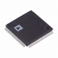
ADUC7129BSTZ126-RL Analog Devices Inc, ADUC7129BSTZ126-RL Datasheet - Page 32

ADUC7129BSTZ126-RL
Manufacturer Part Number
ADUC7129BSTZ126-RL
Description
IC DAS MCU ARM7 ADC/DDS 80-LQFP
Manufacturer
Analog Devices Inc
Series
MicroConverter® ADuC7xxxr
Datasheet
1.EVAL-ADUC7128QSPZ.pdf
(92 pages)
Specifications of ADUC7129BSTZ126-RL
Core Size
16/32-Bit
Program Memory Size
126KB (126K x 8)
Core Processor
ARM7
Speed
41.78MHz
Connectivity
EBI/EMI, I²C, SPI, UART/USART
Peripherals
PLA, POR, PWM, PSM, Temp Sensor, WDT
Number Of I /o
38
Program Memory Type
FLASH
Ram Size
8K x 8
Voltage - Supply (vcc/vdd)
3 V ~ 3.6 V
Data Converters
A/D 10x12b; D/A 1x10b
Oscillator Type
Internal
Operating Temperature
-40°C ~ 125°C
Package / Case
80-LQFP
Controller Family/series
(ARM7) ADUC
No. Of I/o's
40
Cpu Speed
41.78MHz
No. Of Timers
5
Digital Ic Case Style
LQFP
Embedded Interface Type
I2C, SPI, UART
Rohs Compliant
Yes
Lead Free Status / RoHS Status
Lead free / RoHS Compliant
Eeprom Size
-
Lead Free Status / RoHS Status
Lead free / RoHS Compliant, Lead free / RoHS Compliant
Other names
ADUC7129BSTZ126-RLTR
Available stocks
Company
Part Number
Manufacturer
Quantity
Price
Company:
Part Number:
ADUC7129BSTZ126-RL
Manufacturer:
Analog Devices Inc
Quantity:
10 000
ADuC7128/ADuC7129
ADC CIRCUIT OVERVIEW
The analog-to-digital converter (ADC) incorporates a fast,
multichannel, 12-bit ADC. It can operate from 3.0 V to 3.6 V
supplies and is capable of providing a throughput of up to 1 MSPS
when the clock source is 41.78 MHz. This block provides the
user with a multichannel multiplexer, differential track-and-
hold, on-chip reference, and ADC.
The ADC consists of a 12-bit successive approximation converter
based around two capacitor DACs. Depending on the input
signal configuration, the ADC can operate in one of the
following three modes:
•
•
•
The converter accepts an analog input range of 0 to V
operating in single-ended mode or pseudo differential mode. In
fully differential mode, the input signal must be balanced around
a common-mode voltage V
with a maximum amplitude of 2 V
A high precision, low drift, and factory-calibrated 2.5 V reference
is provided on-chip. An external reference can also be connected
as described in the Band Gap Reference section.
Single or continuous conversion modes can be initiated in software.
An external CONVST pin, an output generated from the on-chip
PLA, a Timer0, or a Timer1 overflow can also be used to
generate a repetitive trigger for ADC conversions.
If the signal has not been deasserted by the time the ADC
conversion is complete, a second conversion begins auto-
matically.
A voltage output from an on-chip band gap reference propor-
tional to absolute temperature can also be routed through the
front-end ADC multiplexer, effectively an additional ADC
channel input. This facilitates an internal temperature sensor
channel, measuring die temperature to an accuracy of ±3°C.
Figure 32. Examples of Balanced Signals for Fully Differential Mode
Fully differential mode, for small and balanced signals
Single-ended mode, for any single-ended signals
Pseudo differential mode, for any single-ended signals,
taking advantage of the common mode rejection offered by
the pseudo differential input
AV
V
CM
DD
0
V
CM
CM
2V
V
, in the range 0 V to AV
CM
REF
REF
(see Figure 32).
2V
REF
2V
REF
DD
REF
and
when
Rev. 0 | Page 32 of 92
ADC TRANSFER FUNCTION
Pseudo Differential Mode and Single-Ended Mode
In pseudo differential or single-ended mode, the input range is
0 to V
differential and single-ended modes with
The ideal code transitions occur midway between successive
integer LSB values (that is, 1/2 LSB, 3/2 LSBs, 5/2 LSBs, …,
FS – 3/2 LSBs). The ideal input/output transfer characteristic is
shown in Figure 33.
Fully Differential Mode
The amplitude of the differential signal is the difference
between the signals applied to the V
V
is, therefore, −V
the common mode (CM). The common mode is the average of
the two signals (V
which the two inputs are centered. This results in the span of
each input being CM ± V
nally, and its range varies with V
Inputs section).
The output coding is twos complement in fully differential
mode with 1 LSB = 2 V
when V
shifted by one to the right. This allows the result in ADCDAT to
be declared as a signed integer when writing C code. The
designed code transitions occur midway between successive
integer LSB values (that is, 1/2 LSB, 3/2 LSBs, 5/2 LSBs, …,
FS − 3/2 LSBs). The ideal input/output transfer characteristic is
shown in Figure 34.
IN+
− V
1 LSB = FS/4096 or
2.5 V/4096 = 0.61 mV or
610 μV when V
1111 1111 1111
1111 1111 1110
1111 1111 1101
1111 1111 1100
0000 0000 0011
0000 0000 0010
0000 0000 0001
0000 0000 0000
Figure 33. ADC Transfer Function in Pseudo Differential Mode or
REF
REF
IN−
. The output coding is straight binary in pseudo
). The maximum amplitude of the differential signal
= 2.5 V. The output result is ±11 bits, but this is
REF
IN+
0V
to +V
+ V
REF
1LSB
1LSB =
IN−
REF
= 2.5 V
Single-Ended Mode
REF
REF
)/2, and is, therefore, the voltage upon
/4096 or 2 × 2.5 V/4096 = 1.22 mV
/2. This voltage has to be set up exter-
p-p (2 × V
4096
FS
VOLTAGE INPUT
REF
(see the Driving the Analog
IN+
REF
and V
). This is regardless of
IN−
pins (that is,
+FS – 1LSB


