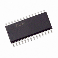
Z8F0431SJ020SG Zilog, Z8F0431SJ020SG Datasheet - Page 128

Z8F0431SJ020SG
Manufacturer Part Number
Z8F0431SJ020SG
Description
IC ENCORE XP MCU FLASH 4K 28SOIC
Manufacturer
Zilog
Series
Encore!®r
Specifications of Z8F0431SJ020SG
Core Processor
Z8
Core Size
8-Bit
Speed
20MHz
Peripherals
Brown-out Detect/Reset, LED, POR, PWM, WDT
Number Of I /o
25
Program Memory Size
4KB (4K x 8)
Program Memory Type
FLASH
Ram Size
256 x 8
Voltage - Supply (vcc/vdd)
2.7 V ~ 3.6 V
Oscillator Type
Internal
Operating Temperature
0°C ~ 70°C
Package / Case
28-SOIC (7.5mm Width)
For Use With
770-1002 - ISP 4PORT ZILOG Z8 ENCORE! MCU
Lead Free Status / RoHS Status
Lead free / RoHS Compliant
Eeprom Size
-
Data Converters
-
Connectivity
-
Other names
269-4627-5
Available stocks
Company
Part Number
Manufacturer
Quantity
Price
Company:
Part Number:
Z8F0431SJ020SG
Manufacturer:
Zilog
Quantity:
784
- Current page: 128 of 251
- Download datasheet (4Mb)
Flash Option Bit Control Register Definitions
PS025111-1207
Note:
Option Bit Types
Trim Bit Address Register
User Option Bits
The user option bits are contained in the first two bytes of program memory. User access
to these bits is provided because these locations contain application specific device
configurations. The information contained here is lost when page 0 of the program
memory is erased.
Trim Option Bits
The trim option bits are contained in the information page of the Flash memory. These bits
are factory programmed values required to optimize the operation of onboard analog
circuitry and cannot be permanently altered by the user. Program memory may be erased
without endangering these values. It is possible to alter working values of these bits by
accessing the trim bit address and data registers, but these working values are lost after a
power loss.
There are 32 bytes of trim data. To modify one of these values, the user code must first
write a value between
trim bit data register changes the working value of the target trim data byte.
Reading the trim data requires the user code to write a value between
trim bit address register. The next read from the trim bit data register returns the working
value of the target trim data byte.
The trim address range is from information address
information page is not accessible through the trim bit address and data registers.
During reset, the first 43 system clock cycles perform 43 Flash accesses. The six bits of
the counter provide the lower six bits of the Flash memory address. All other address bits
are set to 0. The option bit registers use the 6-bit address from the counter as an address
and latch the data from the Flash on the positive edge of the IPO clock, allowing for a
maximum of 344-bits (43 bytes) of option information to be read from the Flash.
Because option information is stored in both the first two bytes of program memory and in
the information area of the Flash, the data must be placed in specific locations to be read
correctly. In this case, the first two bytes at address 0 and 1 in the program memory are
read out, and the rest of the bytes are read-out of the information part of the Flash.
This register contains the target address to access the trim option bits.Trim bit address
(
00h-1Fh
) maps to the information area address (
00H
and
1FH
into the trim bit address register. The next write to the
20h-3Fh
20-3F
Z8 Encore!
) as listed in
Product Specification
only. The remaining
00H
Table
®
and
Flash Option Bits
F0830 Series
1FH
77.
into the
118
Related parts for Z8F0431SJ020SG
Image
Part Number
Description
Manufacturer
Datasheet
Request
R

Part Number:
Description:
Communication Controllers, ZILOG INTELLIGENT PERIPHERAL CONTROLLER (ZIP)
Manufacturer:
Zilog, Inc.
Datasheet:

Part Number:
Description:
KIT DEV FOR Z8 ENCORE 16K TO 64K
Manufacturer:
Zilog
Datasheet:

Part Number:
Description:
KIT DEV Z8 ENCORE XP 28-PIN
Manufacturer:
Zilog
Datasheet:

Part Number:
Description:
DEV KIT FOR Z8 ENCORE 8K/4K
Manufacturer:
Zilog
Datasheet:

Part Number:
Description:
KIT DEV Z8 ENCORE XP 28-PIN
Manufacturer:
Zilog
Datasheet:

Part Number:
Description:
DEV KIT FOR Z8 ENCORE 4K TO 8K
Manufacturer:
Zilog
Datasheet:

Part Number:
Description:
CMOS Z8 microcontroller. ROM 16 Kbytes, RAM 256 bytes, speed 16 MHz, 32 lines I/O, 3.0V to 5.5V
Manufacturer:
Zilog, Inc.
Datasheet:

Part Number:
Description:
Low-cost microcontroller. 512 bytes ROM, 61 bytes RAM, 8 MHz
Manufacturer:
Zilog, Inc.
Datasheet:

Part Number:
Description:
Z8 4K OTP Microcontroller
Manufacturer:
Zilog, Inc.
Datasheet:

Part Number:
Description:
CMOS SUPER8 ROMLESS MCU
Manufacturer:
Zilog, Inc.
Datasheet:

Part Number:
Description:
SL1866 CMOSZ8 OTP Microcontroller
Manufacturer:
Zilog, Inc.
Datasheet:

Part Number:
Description:
SL1866 CMOSZ8 OTP Microcontroller
Manufacturer:
Zilog, Inc.
Datasheet:

Part Number:
Description:
OTP (KB) = 1, RAM = 125, Speed = 12, I/O = 14, 8-bit Timers = 2, Comm Interfaces Other Features = Por, LV Protect, Voltage = 4.5-5.5V
Manufacturer:
Zilog, Inc.
Datasheet:

Part Number:
Description:
Manufacturer:
Zilog, Inc.
Datasheet:


