Z8F0431SJ020SG Zilog, Z8F0431SJ020SG Datasheet - Page 55
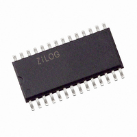
Z8F0431SJ020SG
Manufacturer Part Number
Z8F0431SJ020SG
Description
IC ENCORE XP MCU FLASH 4K 28SOIC
Manufacturer
Zilog
Series
Encore!®r
Specifications of Z8F0431SJ020SG
Core Processor
Z8
Core Size
8-Bit
Speed
20MHz
Peripherals
Brown-out Detect/Reset, LED, POR, PWM, WDT
Number Of I /o
25
Program Memory Size
4KB (4K x 8)
Program Memory Type
FLASH
Ram Size
256 x 8
Voltage - Supply (vcc/vdd)
2.7 V ~ 3.6 V
Oscillator Type
Internal
Operating Temperature
0°C ~ 70°C
Package / Case
28-SOIC (7.5mm Width)
For Use With
770-1002 - ISP 4PORT ZILOG Z8 ENCORE! MCU
Lead Free Status / RoHS Status
Lead free / RoHS Compliant
Eeprom Size
-
Data Converters
-
Connectivity
-
Other names
269-4627-5
Available stocks
Company
Part Number
Manufacturer
Quantity
Price
Company:

Part Number:
Z8F0431SJ020SG
Manufacturer:
Zilog
Quantity:
784


Table 17. Port A–D Control Registers (PxCTL)
Table 18. Port A–D Data Direction Sub-Registers (PxDD)
BITS
FIELD
RESET
R/W
ADDR
BITS
FIELD
RESET
R/W
ADDR
PS025111-1207
Port A–D Data Direction Subregisters
Port A–D Alternate Function Subregisters
DD7
R/W
R/W
If 01H in Port A–D Address Register, accessible through the Port A–D Control Register
7
7
1
PCTL[7:0]—Port Control
The port control register provides access to all subregisters that configure the GPIO port
operation.
The Port A–D data direction subregister is accessed through the Port A–D control register
by writing 01H to the Port A–D address register. See
DD[7:0]—Data direction
These bits control the direction of the associated port pin. Port Alternate Function
operation overrides the Data direction register setting.
0 = Output. Data in the Port A–D output data register is driven onto the port pin.
1 = Input. The port pin is sampled and the value written into the Port A–D input data
register. The output driver is tristated.
The Port A–D Alternate function subregister is accessed through the Port A–D control
register by writing
Port A–D Alternate function subregisters enable the Alternate function selection on pins.
If disabled, the pins functions as GPIO. If enabled, select one of four Alternate functions
using Alternate function set subregisters 1 and 2 as described in the
Function Set 1 Subregisters
Subregisters
Alternate functions associated with each port pin.
R/W
DD6
R/W
6
6
1
on page 49
02H
DD5
R/W
R/W
5
5
1
to the Port A–D address register. See
.
See
FD1H, FD5H, FD9H, FDDH
on page 48 and
GPIO Alternate Functions
R/W
DD4
R/W
4
4
1
PCTL
00H
Port A–D Alternate Function Set 2
DD3
R/W
R/W
3
3
1
Table
on page 38 to determine the
R/W
DD2
R/W
18.
Z8 Encore!
2
2
1
Table 19
General Purpose Input/Output
Product Specification
Port A–D Alternate
DD1
R/W
R/W
on page 46. The
1
1
1
®
F0830 Series
R/W
DD0
R/W
0
0
1
45
Related parts for Z8F0431SJ020SG
Image
Part Number
Description
Manufacturer
Datasheet
Request
R

Part Number:
Description:
Communication Controllers, ZILOG INTELLIGENT PERIPHERAL CONTROLLER (ZIP)
Manufacturer:
Zilog, Inc.
Datasheet:

Part Number:
Description:
KIT DEV FOR Z8 ENCORE 16K TO 64K
Manufacturer:
Zilog
Datasheet:

Part Number:
Description:
KIT DEV Z8 ENCORE XP 28-PIN
Manufacturer:
Zilog
Datasheet:

Part Number:
Description:
DEV KIT FOR Z8 ENCORE 8K/4K
Manufacturer:
Zilog
Datasheet:

Part Number:
Description:
KIT DEV Z8 ENCORE XP 28-PIN
Manufacturer:
Zilog
Datasheet:

Part Number:
Description:
DEV KIT FOR Z8 ENCORE 4K TO 8K
Manufacturer:
Zilog
Datasheet:
Part Number:
Description:
CMOS Z8 microcontroller. ROM 16 Kbytes, RAM 256 bytes, speed 16 MHz, 32 lines I/O, 3.0V to 5.5V
Manufacturer:
Zilog, Inc.
Datasheet:
Part Number:
Description:
Low-cost microcontroller. 512 bytes ROM, 61 bytes RAM, 8 MHz
Manufacturer:
Zilog, Inc.
Datasheet:
Part Number:
Description:
Z8 4K OTP Microcontroller
Manufacturer:
Zilog, Inc.
Datasheet:
Part Number:
Description:
CMOS SUPER8 ROMLESS MCU
Manufacturer:
Zilog, Inc.
Datasheet:
Part Number:
Description:
SL1866 CMOSZ8 OTP Microcontroller
Manufacturer:
Zilog, Inc.
Datasheet:
Part Number:
Description:
SL1866 CMOSZ8 OTP Microcontroller
Manufacturer:
Zilog, Inc.
Datasheet:
Part Number:
Description:
OTP (KB) = 1, RAM = 125, Speed = 12, I/O = 14, 8-bit Timers = 2, Comm Interfaces Other Features = Por, LV Protect, Voltage = 4.5-5.5V
Manufacturer:
Zilog, Inc.
Datasheet:
Part Number:
Description:
Manufacturer:
Zilog, Inc.
Datasheet: