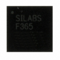
C8051F365-GM Silicon Laboratories Inc, C8051F365-GM Datasheet - Page 90

C8051F365-GM
Manufacturer Part Number
C8051F365-GM
Description
IC 8051 MCU 32K FLASH 28-QFN
Manufacturer
Silicon Laboratories Inc
Series
C8051F36xr
Specifications of C8051F365-GM
Program Memory Type
FLASH
Program Memory Size
32KB (32K x 8)
Package / Case
28-QFN
Core Processor
8051
Core Size
8-Bit
Speed
100MHz
Connectivity
SMBus (2-Wire/I²C), SPI, UART/USART
Peripherals
POR, PWM, Temp Sensor, WDT
Number Of I /o
25
Ram Size
1K x 8
Voltage - Supply (vcc/vdd)
3 V ~ 3.6 V
Oscillator Type
Internal
Operating Temperature
-40°C ~ 85°C
Processor Series
C8051F3x
Core
8051
Data Bus Width
8 bit
Data Ram Size
1 KB
Interface Type
I2C/SMBus/SPI/UART
Maximum Clock Frequency
100 MHz
Number Of Programmable I/os
25
Number Of Timers
4
Maximum Operating Temperature
+ 85 C
Mounting Style
SMD/SMT
3rd Party Development Tools
KSK-SL-TOOLSTICK, PK51, CA51, A51, ULINK2
Development Tools By Supplier
C8051F360DK
Minimum Operating Temperature
- 40 C
Package
28QFN
Device Core
8051
Family Name
C8051F36x
Maximum Speed
100 MHz
Operating Supply Voltage
3.3 V
Lead Free Status / RoHS Status
Lead free / RoHS Compliant
For Use With
770-1006 - ISP 4PORT FOR SILABS C8051F MCU336-1410 - KIT DEV FOR C8051F360 FAMILY
Eeprom Size
-
Data Converters
-
Lead Free Status / Rohs Status
Lead free / RoHS Compliant
Other names
336-1647
Available stocks
Company
Part Number
Manufacturer
Quantity
Price
Part Number:
C8051F365-GM
Manufacturer:
SILICON LABS/èٹ¯ç§‘
Quantity:
20 000
- Current page: 90 of 288
- Download datasheet (3Mb)
C8051F360/1/2/3/4/5/6/7/8/9
9.4.6.3. SFR Page Stack Example
The following is an example that shows the operation of the SFR Page Stack during interrupts.
In this example, the SFR Page Control is left in the default enabled state (i.e., SFRPGEN = 1), and the
CIP-51 is executing in-line code that is writing values to OSCICN (SFR “OSCICN”, located at address
0xB6 on SFR Page 0x0F). The device is also using the Programmable Counter Array (PCA) and the 10-bit
ADC (ADC0) window comparator to monitor a voltage. The PCA is timing a critical control function in its
interrupt service routine (ISR), so its interrupt is enabled and is set to high priority. The ADC0 is monitoring
a voltage that is less important, but to minimize the software overhead its window comparator is being used
with an associated ISR that is set to low priority. At this point, the SFR page is set to access the OSCICN
SFR (SFRPAGE = 0x0F). See Figure 9.4 below.
SFR Page
Stack SFR's
0x0F
SFRPAGE
(OSCICN)
SFRNEXT
SFRLAST
Figure 9.4. SFR Page Stack While Using SFR Page 0x0F To Access OSCICN
While CIP-51 executes in-line code (writing values to OSCICN in this example), ADC0 Window Compara-
tor Interrupt occurs. The CIP-51 vectors to the ADC0 Window Comparator ISR and pushes the current
SFR Page value (SFR Page 0x0F) into SFRNEXT in the SFR Page Stack. SFR page 0x00 is then auto-
matically placed in the SFRPAGE register. SFRPAGE is considered the “top” of the SFR Page Stack. Soft-
ware can now access the ADC0 SFR’s. Software may switch to any SFR Page by writing a new value to
the SFRPAGE register at any time during the ADC0 ISR to access SFR’s that are not on SFR Page 0x00.
See Figure 9.5 below.
90
Rev. 1.0
Related parts for C8051F365-GM
Image
Part Number
Description
Manufacturer
Datasheet
Request
R
Part Number:
Description:
SMD/C°/SINGLE-ENDED OUTPUT SILICON OSCILLATOR
Manufacturer:
Silicon Laboratories Inc
Part Number:
Description:
Manufacturer:
Silicon Laboratories Inc
Datasheet:
Part Number:
Description:
N/A N/A/SI4010 AES KEYFOB DEMO WITH LCD RX
Manufacturer:
Silicon Laboratories Inc
Datasheet:
Part Number:
Description:
N/A N/A/SI4010 SIMPLIFIED KEY FOB DEMO WITH LED RX
Manufacturer:
Silicon Laboratories Inc
Datasheet:
Part Number:
Description:
N/A/-40 TO 85 OC/EZLINK MODULE; F930/4432 HIGH BAND (REV E/B1)
Manufacturer:
Silicon Laboratories Inc
Part Number:
Description:
EZLink Module; F930/4432 Low Band (rev e/B1)
Manufacturer:
Silicon Laboratories Inc
Part Number:
Description:
I°/4460 10 DBM RADIO TEST CARD 434 MHZ
Manufacturer:
Silicon Laboratories Inc
Part Number:
Description:
I°/4461 14 DBM RADIO TEST CARD 868 MHZ
Manufacturer:
Silicon Laboratories Inc
Part Number:
Description:
I°/4463 20 DBM RFSWITCH RADIO TEST CARD 460 MHZ
Manufacturer:
Silicon Laboratories Inc
Part Number:
Description:
I°/4463 20 DBM RADIO TEST CARD 868 MHZ
Manufacturer:
Silicon Laboratories Inc
Part Number:
Description:
I°/4463 27 DBM RADIO TEST CARD 868 MHZ
Manufacturer:
Silicon Laboratories Inc
Part Number:
Description:
I°/4463 SKYWORKS 30 DBM RADIO TEST CARD 915 MHZ
Manufacturer:
Silicon Laboratories Inc
Part Number:
Description:
N/A N/A/-40 TO 85 OC/4463 RFMD 30 DBM RADIO TEST CARD 915 MHZ
Manufacturer:
Silicon Laboratories Inc
Part Number:
Description:
I°/4463 20 DBM RADIO TEST CARD 169 MHZ
Manufacturer:
Silicon Laboratories Inc


