DF2378BVFQ35WV Renesas Electronics America, DF2378BVFQ35WV Datasheet - Page 1029
DF2378BVFQ35WV
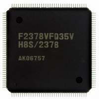
Manufacturer Part Number
DF2378BVFQ35WV
Description
IC H8S/2378 MCU FLASH 144-QFP
Manufacturer
Renesas Electronics America
Series
H8® H8S/2300r
Datasheet
1.YR0K42378FC000BA.pdf
(1208 pages)
Specifications of DF2378BVFQ35WV
Core Processor
H8S/2000
Core Size
16-Bit
Speed
35MHz
Connectivity
I²C, IrDA, SCI, SmartCard
Peripherals
DMA, POR, PWM, WDT
Number Of I /o
97
Program Memory Size
512KB (512K x 8)
Program Memory Type
FLASH
Ram Size
32K x 8
Voltage - Supply (vcc/vdd)
3 V ~ 3.6 V
Data Converters
A/D 16x10b; D/A 6x8b
Oscillator Type
Internal
Operating Temperature
-40°C ~ 85°C
Package / Case
144-QFP
For Use With
EDK2378 - DEV EVAL KIT FOR H8S/2378
Lead Free Status / RoHS Status
Lead free / RoHS Compliant
Eeprom Size
-
Available stocks
Company
Part Number
Manufacturer
Quantity
Price
Company:

Part Number:
DF2378BVFQ35WV
Manufacturer:
Renesas Electronics America
Quantity:
10 000


23.3
The PLL circuit has the function of multiplying the frequency of the clock from the oscillator by a
factor of 1, 2, or 4. The multiplication factor is set with the STC1 and the STC0 bits in PLLCR.
The phase of the rising edge of the internal clock is controlled so as to match that of the rising
edge of the EXTAL pin.
When the multiplication factor of the PLL circuit is changed, the operation varies according to the
setting of the STCS bit in SCKCR.
When STCS = 0, the setting becomes valid after a transition to software standby mode. The
transition time count is performed in accordance with the setting of bits STS3 to STS0 in SBYCR.
For details on SBYCR, refer to section 24.1.1, Standby Control Register (SBYCR).
1. The initial PLL circuit multiplication factor is 1.
2. A value is set in bits STS3 to STS0 to give the specified transition time.
3. The target value is set in bits STC1 and STC0, and a transition is made to software standby
4. The clock pulse generator stops and the value set in STC1 and STC0 becomes valid.
5. Software standby mode is cleared, and a transition time is secured in accordance with the
6. After the set transition time has elapsed, this LSI resumes operation using the target
When STCS = 1, this LSI operates using the new multiplication factor immediately after bits
STC1 and STC0 are rewritten.
23.4
The frequency divider divides the PLL output clock to generate a 1/2, 1/4, or 1/8 clock.
mode.
setting in STS3 to STS0.
multiplication factor.
PLL Circuit
Frequency Divider
Rev.7.00 Mar. 18, 2009 page 961 of 1136
Section 23 Clock Pulse Generator
REJ09B0109-0700
Related parts for DF2378BVFQ35WV
Image
Part Number
Description
Manufacturer
Datasheet
Request
R

Part Number:
Description:
KIT STARTER FOR M16C/29
Manufacturer:
Renesas Electronics America
Datasheet:

Part Number:
Description:
KIT STARTER FOR R8C/2D
Manufacturer:
Renesas Electronics America
Datasheet:

Part Number:
Description:
R0K33062P STARTER KIT
Manufacturer:
Renesas Electronics America
Datasheet:

Part Number:
Description:
KIT STARTER FOR R8C/23 E8A
Manufacturer:
Renesas Electronics America
Datasheet:

Part Number:
Description:
KIT STARTER FOR R8C/25
Manufacturer:
Renesas Electronics America
Datasheet:

Part Number:
Description:
KIT STARTER H8S2456 SHARPE DSPLY
Manufacturer:
Renesas Electronics America
Datasheet:

Part Number:
Description:
KIT STARTER FOR R8C38C
Manufacturer:
Renesas Electronics America
Datasheet:

Part Number:
Description:
KIT STARTER FOR R8C35C
Manufacturer:
Renesas Electronics America
Datasheet:

Part Number:
Description:
KIT STARTER FOR R8CL3AC+LCD APPS
Manufacturer:
Renesas Electronics America
Datasheet:
Part Number:
Description:
KIT STARTER FOR RX610
Manufacturer:
Renesas Electronics America
Datasheet:

Part Number:
Description:
KIT STARTER FOR R32C/118
Manufacturer:
Renesas Electronics America
Datasheet:

Part Number:
Description:
KIT DEV RSK-R8C/26-29
Manufacturer:
Renesas Electronics America
Datasheet:

Part Number:
Description:
KIT STARTER FOR SH7124
Manufacturer:
Renesas Electronics America
Datasheet:

Part Number:
Description:
KIT STARTER FOR H8SX/1622
Manufacturer:
Renesas Electronics America
Datasheet:

Part Number:
Description:
KIT DEV FOR SH7203
Manufacturer:
Renesas Electronics America
Datasheet: