DF2378BVFQ35WV Renesas Electronics America, DF2378BVFQ35WV Datasheet - Page 320
DF2378BVFQ35WV
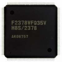
Manufacturer Part Number
DF2378BVFQ35WV
Description
IC H8S/2378 MCU FLASH 144-QFP
Manufacturer
Renesas Electronics America
Series
H8® H8S/2300r
Datasheet
1.YR0K42378FC000BA.pdf
(1208 pages)
Specifications of DF2378BVFQ35WV
Core Processor
H8S/2000
Core Size
16-Bit
Speed
35MHz
Connectivity
I²C, IrDA, SCI, SmartCard
Peripherals
DMA, POR, PWM, WDT
Number Of I /o
97
Program Memory Size
512KB (512K x 8)
Program Memory Type
FLASH
Ram Size
32K x 8
Voltage - Supply (vcc/vdd)
3 V ~ 3.6 V
Data Converters
A/D 16x10b; D/A 6x8b
Oscillator Type
Internal
Operating Temperature
-40°C ~ 85°C
Package / Case
144-QFP
For Use With
EDK2378 - DEV EVAL KIT FOR H8S/2378
Lead Free Status / RoHS Status
Lead free / RoHS Compliant
Eeprom Size
-
Available stocks
Company
Part Number
Manufacturer
Quantity
Price
Company:

Part Number:
DF2378BVFQ35WV
Manufacturer:
Renesas Electronics America
Quantity:
10 000


Section 6 Bus Controller (BSC)
Relationship between Chip Select (CS) Signal and Read (RD) Signal: Depending on the
system’s load conditions, the RD signal may lag behind the CS signal. An example is shown in
figure 6.68. In this case, with the setting for no idle cycle insertion (a), there may be a period of
overlap between the bus cycle A RD signal and the bus cycle B CS signal. Setting idle cycle
insertion, as in (b), however, will prevent any overlap between the RD and CS signals. In the
initial state after reset release, idle cycle insertion (b) is set.
Rev.7.00 Mar. 18, 2009 page 252 of 1136
REJ09B0109-0700
Address bus
CS (area A)
CS (area B)
Figure 6.68 Relationship between Chip Select (CS) and Read (RD)
RD
Overlap period between CS (area B)
and RD may occur
φ
(a) No idle cycle insertion
T
(ICIS1 = 0)
1
Bus cycle A
T
2
T
3
Bus cycle B
T
1
T
2
Address bus
CS (area A)
CS (area B)
RD
φ
T
(b) Idle cycle insertion
1
Bus cycle A
(ICIS1 = 1, initial value)
T
2
T
3
Idle cycle
T
i
Bus cycle B
T
1
T
2
Related parts for DF2378BVFQ35WV
Image
Part Number
Description
Manufacturer
Datasheet
Request
R

Part Number:
Description:
KIT STARTER FOR M16C/29
Manufacturer:
Renesas Electronics America
Datasheet:

Part Number:
Description:
KIT STARTER FOR R8C/2D
Manufacturer:
Renesas Electronics America
Datasheet:

Part Number:
Description:
R0K33062P STARTER KIT
Manufacturer:
Renesas Electronics America
Datasheet:

Part Number:
Description:
KIT STARTER FOR R8C/23 E8A
Manufacturer:
Renesas Electronics America
Datasheet:

Part Number:
Description:
KIT STARTER FOR R8C/25
Manufacturer:
Renesas Electronics America
Datasheet:

Part Number:
Description:
KIT STARTER H8S2456 SHARPE DSPLY
Manufacturer:
Renesas Electronics America
Datasheet:

Part Number:
Description:
KIT STARTER FOR R8C38C
Manufacturer:
Renesas Electronics America
Datasheet:

Part Number:
Description:
KIT STARTER FOR R8C35C
Manufacturer:
Renesas Electronics America
Datasheet:

Part Number:
Description:
KIT STARTER FOR R8CL3AC+LCD APPS
Manufacturer:
Renesas Electronics America
Datasheet:
Part Number:
Description:
KIT STARTER FOR RX610
Manufacturer:
Renesas Electronics America
Datasheet:

Part Number:
Description:
KIT STARTER FOR R32C/118
Manufacturer:
Renesas Electronics America
Datasheet:

Part Number:
Description:
KIT DEV RSK-R8C/26-29
Manufacturer:
Renesas Electronics America
Datasheet:

Part Number:
Description:
KIT STARTER FOR SH7124
Manufacturer:
Renesas Electronics America
Datasheet:

Part Number:
Description:
KIT STARTER FOR H8SX/1622
Manufacturer:
Renesas Electronics America
Datasheet:

Part Number:
Description:
KIT DEV FOR SH7203
Manufacturer:
Renesas Electronics America
Datasheet: