DF2378BVFQ35WV Renesas Electronics America, DF2378BVFQ35WV Datasheet - Page 94
DF2378BVFQ35WV
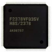
Manufacturer Part Number
DF2378BVFQ35WV
Description
IC H8S/2378 MCU FLASH 144-QFP
Manufacturer
Renesas Electronics America
Series
H8® H8S/2300r
Datasheet
1.YR0K42378FC000BA.pdf
(1208 pages)
Specifications of DF2378BVFQ35WV
Core Processor
H8S/2000
Core Size
16-Bit
Speed
35MHz
Connectivity
I²C, IrDA, SCI, SmartCard
Peripherals
DMA, POR, PWM, WDT
Number Of I /o
97
Program Memory Size
512KB (512K x 8)
Program Memory Type
FLASH
Ram Size
32K x 8
Voltage - Supply (vcc/vdd)
3 V ~ 3.6 V
Data Converters
A/D 16x10b; D/A 6x8b
Oscillator Type
Internal
Operating Temperature
-40°C ~ 85°C
Package / Case
144-QFP
For Use With
EDK2378 - DEV EVAL KIT FOR H8S/2378
Lead Free Status / RoHS Status
Lead free / RoHS Compliant
Eeprom Size
-
Available stocks
Company
Part Number
Manufacturer
Quantity
Price
Company:

Part Number:
DF2378BVFQ35WV
Manufacturer:
Renesas Electronics America
Quantity:
10 000


Section 1 Overview
Rev.7.00 Mar. 18, 2009 page 26 of 1136
REJ09B0109-0700
Type
Bus
control
Interrupt
signals
Symbol
OE
(OE)
CKE *
(CKE) *
NMI
IRQ15 to
IRQ0
(IRQ15) to
(IRQ0)
1
1
H8S/2378
0.18μm
F-ZTAT Group,
H8S/2378R
0.18μm
F-ZTAT Group
(LQFP-144)
38,
137
38,
137
40
86, 85,
106 to 104,
83 to 81,
31 to 28,
136 to 133
58 to 51,
38, 37,
61 to 59,
34, 33, 3
H8S/2378
0.18μm
F-ZTAT Group,
H8S/2378R
0.18μm
F-ZTAT Group
(LGA-145)
M2,
A5
M2,
A5
N1
H10, H12,
C13, C12,
D10, J10,
K13, J12,
J3, K2, J1,
K4, D4, C6,
B5, A6
M8, N7, K8,
K7, K6, N6,
M7, L6, M2,
N2, N8, K9,
L7, K3, L2, C2
Pin No.
H8S/2377
H8S/2377R
38,
137
38,
137
40
86, 85,
106 to 104,
83 to 81,
31 to 28,
136 to 133
58 to 51,
38, 37,
61 to 59,
34, 33, 3
H8S/2375
H8S/2373
H8S/2375R
H8S/2373R I/O
38,
137
38,
137
40
86, 85,
106 to 104,
83 to 81,
31 to 28,
136 to 133
58 to 51,
38, 37,
61 to 59,
34, 33, 3
Output Output enable
Output Clock enable signal
Input
Input
Function
signal for DRAM
interface space.
The output pins of
OE and (OE) are
selected by the port
function control
register 2 (PFCR2)
of port 3.
of the synchronous
DRAM interface
space.
The output pins of
CKE and (CKE) are
selected by the port
function control
register 2 (PFCR2)
of port 3.
Nonmaskable
interrupt request
pin. Fix high when
not used.
These pins request
a maskable
interrupt.
The input pins of
IRQn and (IRQn)
are selected by the
IRQ pin select
register (ITSR) of
the interrupt
controller.
(n = 0 to 15)
Related parts for DF2378BVFQ35WV
Image
Part Number
Description
Manufacturer
Datasheet
Request
R

Part Number:
Description:
KIT STARTER FOR M16C/29
Manufacturer:
Renesas Electronics America
Datasheet:

Part Number:
Description:
KIT STARTER FOR R8C/2D
Manufacturer:
Renesas Electronics America
Datasheet:

Part Number:
Description:
R0K33062P STARTER KIT
Manufacturer:
Renesas Electronics America
Datasheet:

Part Number:
Description:
KIT STARTER FOR R8C/23 E8A
Manufacturer:
Renesas Electronics America
Datasheet:

Part Number:
Description:
KIT STARTER FOR R8C/25
Manufacturer:
Renesas Electronics America
Datasheet:

Part Number:
Description:
KIT STARTER H8S2456 SHARPE DSPLY
Manufacturer:
Renesas Electronics America
Datasheet:

Part Number:
Description:
KIT STARTER FOR R8C38C
Manufacturer:
Renesas Electronics America
Datasheet:

Part Number:
Description:
KIT STARTER FOR R8C35C
Manufacturer:
Renesas Electronics America
Datasheet:

Part Number:
Description:
KIT STARTER FOR R8CL3AC+LCD APPS
Manufacturer:
Renesas Electronics America
Datasheet:
Part Number:
Description:
KIT STARTER FOR RX610
Manufacturer:
Renesas Electronics America
Datasheet:

Part Number:
Description:
KIT STARTER FOR R32C/118
Manufacturer:
Renesas Electronics America
Datasheet:

Part Number:
Description:
KIT DEV RSK-R8C/26-29
Manufacturer:
Renesas Electronics America
Datasheet:

Part Number:
Description:
KIT STARTER FOR SH7124
Manufacturer:
Renesas Electronics America
Datasheet:

Part Number:
Description:
KIT STARTER FOR H8SX/1622
Manufacturer:
Renesas Electronics America
Datasheet:

Part Number:
Description:
KIT DEV FOR SH7203
Manufacturer:
Renesas Electronics America
Datasheet: