DF2378BVFQ35WV Renesas Electronics America, DF2378BVFQ35WV Datasheet - Page 15
DF2378BVFQ35WV
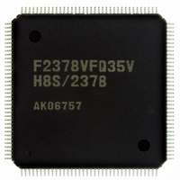
Manufacturer Part Number
DF2378BVFQ35WV
Description
IC H8S/2378 MCU FLASH 144-QFP
Manufacturer
Renesas Electronics America
Series
H8® H8S/2300r
Datasheet
1.YR0K42378FC000BA.pdf
(1208 pages)
Specifications of DF2378BVFQ35WV
Core Processor
H8S/2000
Core Size
16-Bit
Speed
35MHz
Connectivity
I²C, IrDA, SCI, SmartCard
Peripherals
DMA, POR, PWM, WDT
Number Of I /o
97
Program Memory Size
512KB (512K x 8)
Program Memory Type
FLASH
Ram Size
32K x 8
Voltage - Supply (vcc/vdd)
3 V ~ 3.6 V
Data Converters
A/D 16x10b; D/A 6x8b
Oscillator Type
Internal
Operating Temperature
-40°C ~ 85°C
Package / Case
144-QFP
For Use With
EDK2378 - DEV EVAL KIT FOR H8S/2378
Lead Free Status / RoHS Status
Lead free / RoHS Compliant
Eeprom Size
-
Available stocks
Company
Part Number
Manufacturer
Quantity
Price
Company:

Part Number:
DF2378BVFQ35WV
Manufacturer:
Renesas Electronics America
Quantity:
10 000


Item
15.4.4 SCI
Initialization
(Asynchronous Mode)
15.6.2 SCI
Initialization (Clocked
Synchronous Mode)
Section 16 I
Interface 2 (IIC2)
(Option)
16.3.1 I
Register A (ICCRA)
Table 16.2 Transfer
Rate
2
C Bus Control
2
C Bus
Page
727
741
771
776
Revision (See Manual for Details)
Description added
Before transmitting and receiving data, you should first clear the
TE and RE bits in SCR to 0, then initialize the SCI as shown in
figure 15.5. Do not write to SMR, SCMR, IrCR, or SEMR while
the SCI is operating. This also applies to writing the same data
as the current register contents. …
Description added
Before transmitting and receiving data, you should first clear the
TE and RE bits in SCR to 0, then initialize the SCI as described
in a sample flowchart in figure 15.15. Do not write to SMR,
SCMR, IrCR, or SEMR while the SCI is operating. This also
applies to writing the same data as the current register contents.
…
Description amended
The I
NXP Semiconductors I
standard and fast mode functions. The register configuration
that controls the I
Semiconductors configuration, however.
Table amended
Notes 3 and 4 added
3. I
4. Due to load conditions, etc., it may not be possible to attain
Bit 3
CKS3 CKS2 CKS1 CKS0 Clock
0*
4
kHz, fast mode: max. 400 kHz).
the specified transfer rate when CKS3 and CKS2 are both
cleared to 0 (bit period: 7.5 tcyc) and the operating
frequency is 20 MHz or higher. Use a bit period other than
7.5 tcyc when the operating frequency exceeds 20 MHz.
Bit 2
0*
2
2
C bus interface specification (standard mode: max. 100
4
C bus interface conforms to and provides a subset of the
Bit 1
0
1
Bit 0
0
1
0
1
φ/28
φ/40
φ/48
φ/64
2
C bus differs partly from the NXP
φ =
8 MHz
286 kHz
200 kHz
167 kHz
125 kHz
2
C bus (inter-IC bus) interface (Rev. 3)
Rev.7.00 Mar. 18, 2009 page xiii of lxvi
φ =
10 MHz
357 kHz
250 kHz
208 kHz
156 kHz
φ =
20 MHz
714 kHz*
500 kHz*
417 kHz*
313 kHz
3
3
3
Transfer Rate
φ =
25 MHz
893 kHz*
625 kHz*
521 kHz*
391 kHz
3
3
3
φ =
33 MHz
1179 kHz*
825 kHz*
688 kHz*
516 kHz*
REJ09B0109-0700
3
3
3
3
φ =
34 MHz*
1214 kHz*
850 kHz*
708 kHz*
531 kHz*
1
3
3
3
3
φ =
35 MHz*
1250 kHz*
875 kHz*
729 kHz*
547 kHz*
2
3
3
3
3
Related parts for DF2378BVFQ35WV
Image
Part Number
Description
Manufacturer
Datasheet
Request
R

Part Number:
Description:
KIT STARTER FOR M16C/29
Manufacturer:
Renesas Electronics America
Datasheet:

Part Number:
Description:
KIT STARTER FOR R8C/2D
Manufacturer:
Renesas Electronics America
Datasheet:

Part Number:
Description:
R0K33062P STARTER KIT
Manufacturer:
Renesas Electronics America
Datasheet:

Part Number:
Description:
KIT STARTER FOR R8C/23 E8A
Manufacturer:
Renesas Electronics America
Datasheet:

Part Number:
Description:
KIT STARTER FOR R8C/25
Manufacturer:
Renesas Electronics America
Datasheet:

Part Number:
Description:
KIT STARTER H8S2456 SHARPE DSPLY
Manufacturer:
Renesas Electronics America
Datasheet:

Part Number:
Description:
KIT STARTER FOR R8C38C
Manufacturer:
Renesas Electronics America
Datasheet:

Part Number:
Description:
KIT STARTER FOR R8C35C
Manufacturer:
Renesas Electronics America
Datasheet:

Part Number:
Description:
KIT STARTER FOR R8CL3AC+LCD APPS
Manufacturer:
Renesas Electronics America
Datasheet:
Part Number:
Description:
KIT STARTER FOR RX610
Manufacturer:
Renesas Electronics America
Datasheet:

Part Number:
Description:
KIT STARTER FOR R32C/118
Manufacturer:
Renesas Electronics America
Datasheet:

Part Number:
Description:
KIT DEV RSK-R8C/26-29
Manufacturer:
Renesas Electronics America
Datasheet:

Part Number:
Description:
KIT STARTER FOR SH7124
Manufacturer:
Renesas Electronics America
Datasheet:

Part Number:
Description:
KIT STARTER FOR H8SX/1622
Manufacturer:
Renesas Electronics America
Datasheet:

Part Number:
Description:
KIT DEV FOR SH7203
Manufacturer:
Renesas Electronics America
Datasheet: