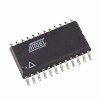
AT90PWM216-16SUR Atmel, AT90PWM216-16SUR Datasheet - Page 248

AT90PWM216-16SUR
Manufacturer Part Number
AT90PWM216-16SUR
Description
MCU AVR 16K FLASH 16MHZ 24SOIC
Manufacturer
Atmel
Series
AVR® 90PWM Lightingr
Datasheet
1.AT90PWM216-16SU.pdf
(359 pages)
Specifications of AT90PWM216-16SUR
Core Processor
AVR
Core Size
8-Bit
Speed
16MHz
Connectivity
SPI, UART/USART
Peripherals
Brown-out Detect/Reset, POR, PWM, WDT
Number Of I /o
19
Program Memory Size
16KB (16K x 8)
Program Memory Type
FLASH
Eeprom Size
512 x 8
Ram Size
1K x 8
Voltage - Supply (vcc/vdd)
2.7 V ~ 5.5 V
Data Converters
A/D 8x10b; D/A 1x10b
Oscillator Type
Internal
Operating Temperature
-40°C ~ 105°C
Package / Case
24-SOIC (7.5mm Width)
Processor Series
AT90PWMx
Core
AVR8
3rd Party Development Tools
EWAVR, EWAVR-BL
Development Tools By Supplier
ATAVRDRAGON, ATSTK500, ATSTK600, ATAVRISP2, ATAVRONEKIT, ATAVRFBKIT, ATAVRISP2
Lead Free Status / RoHS Status
Lead free / RoHS Compliant
- Current page: 248 of 359
- Download datasheet (6Mb)
21.8
21.8.1
248
ADC Register Description
AT90PWM216/316
ADC Multiplexer Register – ADMUX
Table 21-2.
Example 1:
Example 2:
The ADC of the AT90PWM216/316 is controlled through 3 different registers. The ADCSRA and
The ADCSRB registers which are the ADC Control and Status registers, and the ADMUX which
allows to select the Vref source and the channel to be converted.
The conversion result is stored on ADCH and ADCL register which contain respectively the most
significant bits and the less significant bits.
Bit
Read/Write
Initial Value
• Bit 7, 6 – REFS1, 0: ADC Vref Selection Bits
V
V
V
...
V
V
V
...
V
V
V
ADCn
ADCm
ADCm
ADCm
ADCm
ADCm
ADCm
ADCm
ADCm
– ADMUX = 0xED (ADC3 - ADC2, 10x gain, 2.56V reference, left adjusted result)
– Voltage on ADC3 is 300 mV, voltage on ADC2 is 500 mV.
– ADCR = 512 * 10 * (300 - 500) / 2560 = -400 = 0x270
– ADCL will thus read 0x00, and ADCH will read 0x9C.
– ADMUX = 0xFB (ADC3 - ADC2, 1x gain, 2.56V reference, left adjusted result)
– Voltage on ADC3 is 300 mV, voltage on ADC2 is 500 mV.
– ADCR = 512 * 1 * (300 - 500) / 2560 = -41 = 0x029.
– ADCL will thus read 0x40, and ADCH will read 0x0A.
+ 0.999 V
+ 0.998 V
+ 0.001 V
- 0.001 V
- 0.999 V
- V
Writing zero to ADLAR right adjusts the result: ADCL = 0x70, ADCH = 0x02.
Writing zero to ADLAR right adjusts the result: ADCL = 0x00, ADCH = 0x29.
+ V
REF
REF
/GAIN
/GAIN
Correlation Between Input Voltage and Output Codes
REF
REF
REFS1
REF
REF
REF
R/W
7
0
/GAIN
/GAIN
/GAIN
/GAIN
/GAIN
REFS0
R/W
6
0
ADLAR
R/W
Read code
5
0
0x1FE
0x1FF
0x1FF
0x3FF
0x001
0x000
0x201
0x200
...
...
4
0
-
-
Corresponding decimal value
510
1
0
-511
-512
511
511
...
-1
...
MUX3
R/W
3
0
MUX2
R/W
2
0
MUX1
R/W
1
0
MUX0
R/W
0
0
7710E–AVR–08/10
ADMUX
Related parts for AT90PWM216-16SUR
Image
Part Number
Description
Manufacturer
Datasheet
Request
R

Part Number:
Description:
Manufacturer:
Atmel Corporation
Datasheet:

Part Number:
Description:
8-bit Microcontroller with 16K Bytes In-System Programmable flash
Manufacturer:
ATMEL [ATMEL Corporation]
Datasheet:

Part Number:
Description:
MCU AVR 16K ISP FLSH 16MHZ24SOIC
Manufacturer:
Atmel
Datasheet:

Part Number:
Description:
DEV KIT FOR AVR/AVR32
Manufacturer:
Atmel
Datasheet:

Part Number:
Description:
INTERVAL AND WIPE/WASH WIPER CONTROL IC WITH DELAY
Manufacturer:
ATMEL Corporation
Datasheet:

Part Number:
Description:
Low-Voltage Voice-Switched IC for Hands-Free Operation
Manufacturer:
ATMEL Corporation
Datasheet:

Part Number:
Description:
MONOLITHIC INTEGRATED FEATUREPHONE CIRCUIT
Manufacturer:
ATMEL Corporation
Datasheet:

Part Number:
Description:
AM-FM Receiver IC U4255BM-M
Manufacturer:
ATMEL Corporation
Datasheet:

Part Number:
Description:
Monolithic Integrated Feature Phone Circuit
Manufacturer:
ATMEL Corporation
Datasheet:

Part Number:
Description:
Multistandard Video-IF and Quasi Parallel Sound Processing
Manufacturer:
ATMEL Corporation
Datasheet:

Part Number:
Description:
High-performance EE PLD
Manufacturer:
ATMEL Corporation
Datasheet:

Part Number:
Description:
8-bit Flash Microcontroller
Manufacturer:
ATMEL Corporation
Datasheet:


