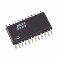
AT90PWM216-16SUR Atmel, AT90PWM216-16SUR Datasheet - Page 254

AT90PWM216-16SUR
Manufacturer Part Number
AT90PWM216-16SUR
Description
MCU AVR 16K FLASH 16MHZ 24SOIC
Manufacturer
Atmel
Series
AVR® 90PWM Lightingr
Datasheet
1.AT90PWM216-16SU.pdf
(359 pages)
Specifications of AT90PWM216-16SUR
Core Processor
AVR
Core Size
8-Bit
Speed
16MHz
Connectivity
SPI, UART/USART
Peripherals
Brown-out Detect/Reset, POR, PWM, WDT
Number Of I /o
19
Program Memory Size
16KB (16K x 8)
Program Memory Type
FLASH
Eeprom Size
512 x 8
Ram Size
1K x 8
Voltage - Supply (vcc/vdd)
2.7 V ~ 5.5 V
Data Converters
A/D 8x10b; D/A 1x10b
Oscillator Type
Internal
Operating Temperature
-40°C ~ 105°C
Package / Case
24-SOIC (7.5mm Width)
Processor Series
AT90PWMx
Core
AVR8
3rd Party Development Tools
EWAVR, EWAVR-BL
Development Tools By Supplier
ATAVRDRAGON, ATSTK500, ATSTK600, ATAVRISP2, ATAVRONEKIT, ATAVRFBKIT, ATAVRISP2
Lead Free Status / RoHS Status
Lead free / RoHS Compliant
- Current page: 254 of 359
- Download datasheet (6Mb)
chronization is done automatically by the ADC interface in such a way that the sample-and-hold
occurs at a specific phase of CK
. A conversion initiated by the user (i.e., all single conver-
ADC2
sions, and the first free running conversion) when CK
is low will take the same amount of
ADC2
time as a single ended conversion (13 ADC clock cycles from the next prescaled clock cycle). A
conversion initiated by the user when CK
is high will take 14 ADC clock cycles due to the
ADC2
synchronization mechanism.
The normal way to use the amplifier is to select a synchronization clock via the AMPxTS1:0 bits
in the AMPxCSR register. Then the amplifier can be switched on, and the amplification is done
on each synchronization event. The amplification is done independently of the ADC.
In order to start an amplified Analog to Digital Conversion on the amplified channel, the ADMUX
must be configured as specified on
Table 21-4 on page
249.
The ADC starting is done by setting the ADSC (ADC Start conversion) bit in the ADCSRB
register.
Until the conversion is not achieved, it is not possible to start a conversion on another channel.
The conversion takes advantage of the amplifier characteristics to ensure minimum conversion
time.
As soon as a conversion is requested thanks to the ADSC bit, the Analog to Digital Conversion
is started. In order to have a better understanding of the functioning of the amplifier synchroniza-
tion, a timing diagram example is shown
Figure
21-15.
In case the amplifier output is modified during the sample phase of the ADC, the on-going con-
version is aborted and restarted as soon as the output of the amplifier is stable as shown
Figure
21-16.
The only precaution to take is to be sure that the trig signal (PSC) frequency is lower than
ADCclk/4.
t is also possible to auto trigger conversion on the amplified channel. In this case, the conversion
is started at the next amplifier clock event following the last auto trigger event selected thanks to
the ADTS bits in the ADCSRB register. In auto trigger conversion, the free running mode is not
possible unless the ADSC bit in ADCSRA is set by soft after each conversion.
Only PSC sources can auto trigger amplified conversion. In this case, the core must have a
clock synchronous with the PSC; if the PSC uses the PLL clock, the core must use PLL/4
clock source.
AT90PWM216/316
254
7710E–AVR–08/10
Related parts for AT90PWM216-16SUR
Image
Part Number
Description
Manufacturer
Datasheet
Request
R

Part Number:
Description:
Manufacturer:
Atmel Corporation
Datasheet:

Part Number:
Description:
8-bit Microcontroller with 16K Bytes In-System Programmable flash
Manufacturer:
ATMEL [ATMEL Corporation]
Datasheet:

Part Number:
Description:
MCU AVR 16K ISP FLSH 16MHZ24SOIC
Manufacturer:
Atmel
Datasheet:

Part Number:
Description:
DEV KIT FOR AVR/AVR32
Manufacturer:
Atmel
Datasheet:

Part Number:
Description:
INTERVAL AND WIPE/WASH WIPER CONTROL IC WITH DELAY
Manufacturer:
ATMEL Corporation
Datasheet:

Part Number:
Description:
Low-Voltage Voice-Switched IC for Hands-Free Operation
Manufacturer:
ATMEL Corporation
Datasheet:

Part Number:
Description:
MONOLITHIC INTEGRATED FEATUREPHONE CIRCUIT
Manufacturer:
ATMEL Corporation
Datasheet:

Part Number:
Description:
AM-FM Receiver IC U4255BM-M
Manufacturer:
ATMEL Corporation
Datasheet:

Part Number:
Description:
Monolithic Integrated Feature Phone Circuit
Manufacturer:
ATMEL Corporation
Datasheet:

Part Number:
Description:
Multistandard Video-IF and Quasi Parallel Sound Processing
Manufacturer:
ATMEL Corporation
Datasheet:

Part Number:
Description:
High-performance EE PLD
Manufacturer:
ATMEL Corporation
Datasheet:

Part Number:
Description:
8-bit Flash Microcontroller
Manufacturer:
ATMEL Corporation
Datasheet:


