AT90PWM216-16SUR Atmel, AT90PWM216-16SUR Datasheet - Page 271
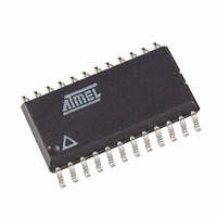
AT90PWM216-16SUR
Manufacturer Part Number
AT90PWM216-16SUR
Description
MCU AVR 16K FLASH 16MHZ 24SOIC
Manufacturer
Atmel
Series
AVR® 90PWM Lightingr
Datasheet
1.AT90PWM216-16SU.pdf
(359 pages)
Specifications of AT90PWM216-16SUR
Core Processor
AVR
Core Size
8-Bit
Speed
16MHz
Connectivity
SPI, UART/USART
Peripherals
Brown-out Detect/Reset, POR, PWM, WDT
Number Of I /o
19
Program Memory Size
16KB (16K x 8)
Program Memory Type
FLASH
Eeprom Size
512 x 8
Ram Size
1K x 8
Voltage - Supply (vcc/vdd)
2.7 V ~ 5.5 V
Data Converters
A/D 8x10b; D/A 1x10b
Oscillator Type
Internal
Operating Temperature
-40°C ~ 105°C
Package / Case
24-SOIC (7.5mm Width)
Processor Series
AT90PWMx
Core
AVR8
3rd Party Development Tools
EWAVR, EWAVR-BL
Development Tools By Supplier
ATAVRDRAGON, ATSTK500, ATSTK600, ATAVRISP2, ATAVRONEKIT, ATAVRFBKIT, ATAVRISP2
Lead Free Status / RoHS Status
Lead free / RoHS Compliant


24.5.1
7710E–AVR–08/10
Store Program Memory Control and Status Register – SPMCSR
Note:
The Store Program Memory Control and Status Register contains the control bits needed to con-
trol the Boot Loader operations.
• Bit 7 – SPMIE: SPM Interrupt Enable
When the SPMIE bit is written to one, and the I-bit in the Status Register is set (one), the SPM
ready interrupt will be enabled. The SPM ready Interrupt will be executed as long as the SPMEN
bit in the SPMCSR Register is cleared.
• Bit 6 – RWWSB: Read-While-Write Section Busy
When a Self-Programming (Page Erase or Page Write) operation to the RWW section is initi-
ated, the RWWSB will be set (one) by hardware. When the RWWSB bit is set, the RWW section
cannot be accessed. The RWWSB bit will be cleared if the RWWSRE bit is written to one after a
Self-Programming operation is completed. Alternatively the RWWSB bit will automatically be
cleared if a page load operation is initiated.
• Bit 5 – Res: Reserved Bit
This bit is a reserved bit in the AT90PWM216/316 and always read as zero.
• Bit 4 – RWWSRE: Read-While-Write Section Read Enable
When programming (Page Erase or Page Write) to the RWW section, the RWW section is
blocked for reading (the RWWSB will be set by hardware). To re-enable the RWW section, the
user software must wait until the programming is completed (SPMEN will be cleared). Then, if
the RWWSRE bit is written to one at the same time as SPMEN, the next SPM instruction within
four clock cycles re-enables the RWW section. The RWW section cannot be re-enabled while
the Flash is busy with a Page Erase or a Page Write (SPMEN is set). If the RWWSRE bit is writ-
ten while the Flash is being loaded, the Flash load operation will abort and the data loaded will
be lost.
• Bit 3 – BLBSET: Boot Lock Bit Set
If this bit is written to one at the same time as SPMEN, the next SPM instruction within four clock
cycles sets Boot Lock bits and Memory Lock bits, according to the data in R0. The data in R1
and the address in the Z-pointer are ignored. The BLBSET bit will automatically be cleared upon
completion of the Lock bit set, or if no SPM instruction is executed within four clock cycles.
An LPM instruction within three cycles after BLBSET and SPMEN are set in the SPMCSR Reg-
ister, will read either the Lock bits or the Fuse bits (depending on Z0 in the Z-pointer) into the
destination register. See
details.
• Bit 2 – PGWRT: Page Write
If this bit is written to one at the same time as SPMEN, the next SPM instruction within four clock
cycles executes Page Write, with the data stored in the temporary buffer. The page address is
taken from the high part of the Z-pointer. The data in R1 and R0 are ignored. The PGWRT bit
Bit
Read/Write
Initial Value
1. “1” means unprogrammed, “0” means programmed
SPMIE
R/W
7
0
RWWSB
R
6
0
“Reading the Fuse and Lock Bits from Software” on page 275
R
5
–
0
RWWSRE
R/W
4
0
BLBSET
R/W
3
0
PGWRT
R/W
2
0
AT90PWM216/316
PGERS
R/W
1
0
SPMEN
R/W
0
0
SPMCSR
271
for
Related parts for AT90PWM216-16SUR
Image
Part Number
Description
Manufacturer
Datasheet
Request
R

Part Number:
Description:
Manufacturer:
Atmel Corporation
Datasheet:

Part Number:
Description:
8-bit Microcontroller with 16K Bytes In-System Programmable flash
Manufacturer:
ATMEL [ATMEL Corporation]
Datasheet:

Part Number:
Description:
MCU AVR 16K ISP FLSH 16MHZ24SOIC
Manufacturer:
Atmel
Datasheet:

Part Number:
Description:
DEV KIT FOR AVR/AVR32
Manufacturer:
Atmel
Datasheet:
Part Number:
Description:
INTERVAL AND WIPE/WASH WIPER CONTROL IC WITH DELAY
Manufacturer:
ATMEL Corporation
Datasheet:
Part Number:
Description:
Low-Voltage Voice-Switched IC for Hands-Free Operation
Manufacturer:
ATMEL Corporation
Datasheet:
Part Number:
Description:
MONOLITHIC INTEGRATED FEATUREPHONE CIRCUIT
Manufacturer:
ATMEL Corporation
Datasheet:
Part Number:
Description:
AM-FM Receiver IC U4255BM-M
Manufacturer:
ATMEL Corporation
Datasheet:
Part Number:
Description:
Monolithic Integrated Feature Phone Circuit
Manufacturer:
ATMEL Corporation
Datasheet:
Part Number:
Description:
Multistandard Video-IF and Quasi Parallel Sound Processing
Manufacturer:
ATMEL Corporation
Datasheet:
Part Number:
Description:
High-performance EE PLD
Manufacturer:
ATMEL Corporation
Datasheet:
Part Number:
Description:
8-bit Flash Microcontroller
Manufacturer:
ATMEL Corporation
Datasheet: