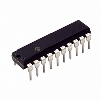
PIC16C781-I/P Microchip Technology, PIC16C781-I/P Datasheet - Page 105

PIC16C781-I/P
Manufacturer Part Number
PIC16C781-I/P
Description
IC MCU OTP 1KX14 W/AD COMP 20DIP
Manufacturer
Microchip Technology
Series
PIC® 16Cr
Datasheets
1.PIC16C781-ISO.pdf
(186 pages)
2.PIC16C781-ISO.pdf
(8 pages)
3.PIC16C781-ISO.pdf
(8 pages)
Specifications of PIC16C781-I/P
Core Size
8-Bit
Program Memory Size
1.75KB (1K x 14)
Core Processor
PIC
Speed
20MHz
Peripherals
Brown-out Detect/Reset, POR, PWM, WDT
Number Of I /o
13
Program Memory Type
OTP
Ram Size
128 x 8
Voltage - Supply (vcc/vdd)
4 V ~ 5.5 V
Data Converters
A/D 8x8b; D/A 1x8b
Oscillator Type
Internal
Operating Temperature
-40°C ~ 85°C
Package / Case
20-DIP (0.300", 7.62mm)
Controller Family/series
PIC16C
No. Of I/o's
16
Ram Memory Size
128Byte
Cpu Speed
20MHz
No. Of Timers
3
Processor Series
PIC16C
Core
PIC
Data Bus Width
8 bit
Data Ram Size
128 B
Maximum Clock Frequency
20 MHz
Number Of Programmable I/os
16
Number Of Timers
2
Operating Supply Voltage
2.5 V to 5.5 V
Maximum Operating Temperature
+ 85 C
Mounting Style
Through Hole
3rd Party Development Tools
52715-96, 52716-328, 52717-734
Development Tools By Supplier
ICE2000, DM163022
Minimum Operating Temperature
- 40 C
On-chip Adc
8 bit
On-chip Dac
8 bit, 1 Channel
Lead Free Status / RoHS Status
Lead free / RoHS Compliant
For Use With
ISPICR1 - ADAPTER IN-CIRCUIT PROGRAMMINGDVA16XP202 - ADAPTER DEVICE PIC16C781/782DM163012 - BOARD DEMO PICDEM FOR 16C781/782AC164028 - MODULE SKT PROMATEII 20SOIC/DIP
Eeprom Size
-
Connectivity
-
Lead Free Status / Rohs Status
Details
Other names
PIC16C781I/P
TABLE 13-4:
Legend: x = Don’t Care
13.1.2
The PSMC has the capability to operate with either a
single output, or dual alternating outputs. In the single
output mode, the PSMC generates an output pulse on
PSMC1A output only. The pulses are at the pro-
grammed frequency, and are variable between the pro-
grammed minimum and maximum duty cycle limits. In
the dual output mode, the PSMC generates output
pulses which alternate between PSMC1A and
PSMC1B. The pulses generated at each output are
generated at one half of the programmed frequency,
and between 50% of the programmed minimum. and
50% maximum of the output duty cycle. The maximum
duty cycle for either output is 50%.
FIGURE 13-4:
Beginning of PSM cycle
During Pulse Duty Cycle
After Pulse Duty Cycle
2001 Microchip Technology Inc.
PWM Signal
on PSMC1A
pin
SC Switch
on PSMC1B
pin
Voltage across C
SINGLE OR DUAL OUTPUT
Time
PSMC1A OUTPUT SEQUENCE IN PSM MODE USING C1 AND C2 COMPARATORS
t = 0
SLOPE COMPENSATION (SC) SWITCH OPERATION
DC = duty cycle
T = Period
0 = Inactive
t = 15/16T
1 = Active
C1OUT
H
L
x
x
x
x
Preliminary
H = High
C2OUT
H
x
L
x
x
x
13.1.3
An optional feature of the PSMC single output mode is
the ability to configure the PSMC1B output for use as a
slope compensation ramp generator. In this mode, the
PSMC1B output is pulled low for the last 1/16 of each
pulse cycle. Connecting the PSMC1B output to an RC
network, similar to Figure 13-4, results in a positive
going pseudo ramp function. This pseudo ramp func-
tion is useful as an offset function for the loop error sig-
nal in unstable conditions at a duty cycle of greater than
50%.
Note:
L = Low
When the Slope Compensation switch is
enabled (SMCOM = 0, and SCEN = 1), the
S1BPOL bit has no effect (see RC Network
on next page for more detail).
SLOPE COMPENSATION
- On
- Off
PIC16C781/782
PSMC1A Output Signal
V
DD
To Slope
Compensation
Circuit
R
V
SS
No Change
No Change
C
150
0
1
0
0
PSMC1A
PSMC1B
1
0
DS41171A-page 103
V
DD
V
PIC16C78X
SS
SC Switch
Module
PSMC


