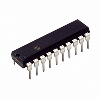
PIC16C781-I/P Microchip Technology, PIC16C781-I/P Datasheet - Page 88

PIC16C781-I/P
Manufacturer Part Number
PIC16C781-I/P
Description
IC MCU OTP 1KX14 W/AD COMP 20DIP
Manufacturer
Microchip Technology
Series
PIC® 16Cr
Datasheets
1.PIC16C781-ISO.pdf
(186 pages)
2.PIC16C781-ISO.pdf
(8 pages)
3.PIC16C781-ISO.pdf
(8 pages)
Specifications of PIC16C781-I/P
Core Size
8-Bit
Program Memory Size
1.75KB (1K x 14)
Core Processor
PIC
Speed
20MHz
Peripherals
Brown-out Detect/Reset, POR, PWM, WDT
Number Of I /o
13
Program Memory Type
OTP
Ram Size
128 x 8
Voltage - Supply (vcc/vdd)
4 V ~ 5.5 V
Data Converters
A/D 8x8b; D/A 1x8b
Oscillator Type
Internal
Operating Temperature
-40°C ~ 85°C
Package / Case
20-DIP (0.300", 7.62mm)
Controller Family/series
PIC16C
No. Of I/o's
16
Ram Memory Size
128Byte
Cpu Speed
20MHz
No. Of Timers
3
Processor Series
PIC16C
Core
PIC
Data Bus Width
8 bit
Data Ram Size
128 B
Maximum Clock Frequency
20 MHz
Number Of Programmable I/os
16
Number Of Timers
2
Operating Supply Voltage
2.5 V to 5.5 V
Maximum Operating Temperature
+ 85 C
Mounting Style
Through Hole
3rd Party Development Tools
52715-96, 52716-328, 52717-734
Development Tools By Supplier
ICE2000, DM163022
Minimum Operating Temperature
- 40 C
On-chip Adc
8 bit
On-chip Dac
8 bit, 1 Channel
Lead Free Status / RoHS Status
Lead free / RoHS Compliant
For Use With
ISPICR1 - ADAPTER IN-CIRCUIT PROGRAMMINGDVA16XP202 - ADAPTER DEVICE PIC16C781/782DM163012 - BOARD DEMO PICDEM FOR 16C781/782AC164028 - MODULE SKT PROMATEII 20SOIC/DIP
Eeprom Size
-
Connectivity
-
Lead Free Status / Rohs Status
Details
Other names
PIC16C781I/P
PIC16C781/782
11.2
The following example demonstrates calibration of the
OPA module as an Operational Amplifier.
EXAMPLE 11-1:
;*
;*
;*
;*
;*
CAL_LOOP
The following example demonstrates how to configure
and calibrate the OPA module as a Voltage Comparator.
EXAMPLE 11-2:
;*
;*
;*
;*
;*
CAL_LOOP
DS41171A-page 86
This code block will configure the OPA
BANKSEL
MOVLW
MOVWF
BCF
BSF
BTFSC
GOTO
MOVLW
BTFSS
CLRW
RETURN
This code block will configure the OPA
Routine returns w=0 if calibration good.
BANKSEL
MOVLW
MOVWF
BSF
MOVLW
MOVWF
MOVLW
MOVWF
BSF
BTFSC
GOTO
MOVLW
BTFSS
CLRW
BSF
RETURN
module as an Op Amp, 2 MHz GBWP, and
calibrated for a common mode voltage of
1.2V. Routine returns w=0 if
calibration good.
module as a voltage comparator, slow
speed, and calibrated for a common mode
voltage of 2.5 V (assumes VDD=5V).
Configuration as OPAMP or
Comparator
OPACON
B’10000001’
OPACON
CALCON,CALREF; Set 1.2V
CALCON,CAL
CALCON,CAL
CAL_LOOP
ERROR_FLAG
CALCON,CALERR; Test for error
OPACON
B’10000000’
OPACON
CALCON,CALREF; Common mode=DAC
H’0x80’
DAC
B’10000000’
DACON0
CALCON,CAL
CALCON,CAL
CAL_LOOP
ERROR_FLAG
CALCON,CALERR; Test for error
OPACON,CMPEN ; Comparator mode
CALIBRATION FOR
OPAMP MODE
CALIBRATION FOR
COMPARATOR MODE
; Op Amp mode &
; Test for end
; Select Bank 2
; 2 MHz GBWP
; Start
; Test for end
; If not, wait
; If no, return 0
; enable DAC,
; VDD ref
; If not, wait
; If no, return 0
; Select Bank 2
; Op Amp mode,
; slow
; DAC at VDD/2
; Start
Preliminary
11.3
A device RESET forces all registers to their RESET
state. This disables the OPA module and clears any
calibration.
11.4
Common AC and DC performance specifications for
the OPA module:
• Common Mode Voltage Range
• Leakage Current
• Input Offset Voltage
• Open Loop Gain
• Gain Bandwidth Product
Common mode voltage range is the specified voltage
range for the OPA+ and OPA- inputs, for which the OPA
module will perform to within its specifications. The
OPA module is designed to operate with input voltages
between 0 and V
voltages greater than V
guaranteed.
Leakage current is a measure of the small source or
sink currents on the OPA+ and OPA- inputs. To mini-
mize the effect of leakage currents, the effective imped-
ances connected to the OPA+ and OPA- inputs should
be kept as small as possible and equal.
Input offset voltage is a measure of the voltage differ-
ence between the OPA+ and OPA- inputs in a closed
loop circuit with the OPA in its linear region. The offset
voltage will appear as a DC offset in the output equal to
the input offset voltage, multiplied by the gain of the cir-
cuit. The input offset voltage is also affected by the
Common mode voltage. The OPA has an automatic
calibration module which can minimize the input offset
voltage of the module.
Open loop gain is the ratio of the output voltage to the
differential input voltage, (OPA+) - (OPA-). The gain is
greatest at DC and falls off with frequency.
Gain Bandwidth Product or GBWP is the frequency
at which the open loop gain falls off to 0 dB. The lower
GBWP is optimized for systems requiring low fre-
quency response and low power consumption.
Effects of RESET
OPA Module Performance
DD
-1.4V. Behavior for Common mode
DD
2001 Microchip Technology Inc.
-1.4V, or below 0V, are not


