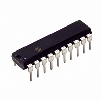
PIC16C781-I/P Microchip Technology, PIC16C781-I/P Datasheet - Page 149

PIC16C781-I/P
Manufacturer Part Number
PIC16C781-I/P
Description
IC MCU OTP 1KX14 W/AD COMP 20DIP
Manufacturer
Microchip Technology
Series
PIC® 16Cr
Datasheets
1.PIC16C781-ISO.pdf
(186 pages)
2.PIC16C781-ISO.pdf
(8 pages)
3.PIC16C781-ISO.pdf
(8 pages)
Specifications of PIC16C781-I/P
Core Size
8-Bit
Program Memory Size
1.75KB (1K x 14)
Core Processor
PIC
Speed
20MHz
Peripherals
Brown-out Detect/Reset, POR, PWM, WDT
Number Of I /o
13
Program Memory Type
OTP
Ram Size
128 x 8
Voltage - Supply (vcc/vdd)
4 V ~ 5.5 V
Data Converters
A/D 8x8b; D/A 1x8b
Oscillator Type
Internal
Operating Temperature
-40°C ~ 85°C
Package / Case
20-DIP (0.300", 7.62mm)
Controller Family/series
PIC16C
No. Of I/o's
16
Ram Memory Size
128Byte
Cpu Speed
20MHz
No. Of Timers
3
Processor Series
PIC16C
Core
PIC
Data Bus Width
8 bit
Data Ram Size
128 B
Maximum Clock Frequency
20 MHz
Number Of Programmable I/os
16
Number Of Timers
2
Operating Supply Voltage
2.5 V to 5.5 V
Maximum Operating Temperature
+ 85 C
Mounting Style
Through Hole
3rd Party Development Tools
52715-96, 52716-328, 52717-734
Development Tools By Supplier
ICE2000, DM163022
Minimum Operating Temperature
- 40 C
On-chip Adc
8 bit
On-chip Dac
8 bit, 1 Channel
Lead Free Status / RoHS Status
Lead free / RoHS Compliant
For Use With
ISPICR1 - ADAPTER IN-CIRCUIT PROGRAMMINGDVA16XP202 - ADAPTER DEVICE PIC16C781/782DM163012 - BOARD DEMO PICDEM FOR 16C781/782AC164028 - MODULE SKT PROMATEII 20SOIC/DIP
Eeprom Size
-
Connectivity
-
Lead Free Status / Rohs Status
Details
Other names
PIC16C781I/P
17.0
Absolute Maximum Ratings †
Ambient temperature under bias....................................................................................................... -55°C to +125°C
Storage temperature ......................................................................................................................... -65°C to +150°C
Voltage on any pin with respect to V
Voltage on V
Maximum voltage between AV
Maximum voltage between AV
Voltage on MCLR with respect to V
Voltage on RA4 with respect to Vss ...................................................................................................0.3 V to +10.5 V
Total power dissipation
Total power dissipation
Maximum current out of V
Maximum current into V
Input clamp current, I
Output clamp current, I
Maximum output current sunk by any I/O pin.................................................................................................... 25 mA
Maximum output current sourced by any I/O pin .............................................................................................. 25 mA
Maximum current sunk by PORTA and PORTB (combined)........................................................................... 200 mA
Maximum current sourced by PORTA and PORTB (combined....................................................................... 200 mA
† NOTICE: Stresses above those listed under “Absolute Maximum Ratings” may cause permanent damage to the
device. This is a stress rating only and functional operation of the device at those or any other conditions above those
indicated in the operation listings of this specification is not implied. Exposure to maximum rating conditions for
extended periods may affect device reliability.
Note 1: Power dissipation is calculated as follows: P
2001 Microchip Technology Inc.
ELECTRICAL CHARACTERISTICS
DD
with respect to V
IK
(1)
(1)
OK
(V
DD
(PDIP, SOIC)............................................................................................................. 1.0 W
(SSOP) .................................................................................................................... 0.65 W
SS
I
(V
< 0 or V
pin ........................................................................................................................ 250 mA
O
pin ..................................................................................................................... 300 mA
DD
SS
< 0 or V
SS
and V
and V
I
SS
.......................................................................................................-0.3 to +7.5 V
SS
> V
................................................................................................ -0.3 V to +8.5 V
O
(except V
SS
DD
DD
> V
pins ............................................................................................... ± 0.3 V
.................................................................................................... ± 20 mA
pins............................................................................................... ± 0.3 V
DD
............................................................................................. ± 20 mA
DD
Preliminary
, MCLR and RA4) ................................... -0.3V to (V
DIS
= V
DD
x {I
DD
-
I
OH
} +
PIC16C781/782
{(V
DD
- V
OH
) x I
DS41171A-page 147
OH
} + (V
DD
+ 0.3 V)
OL
x I
OL
).


