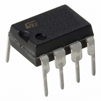
ST7FLITEUS5B6 STMicroelectronics, ST7FLITEUS5B6 Datasheet - Page 109

ST7FLITEUS5B6
Manufacturer Part Number
ST7FLITEUS5B6
Description
MCU 8BIT 1KB FLASH 128KB 8-DIP
Manufacturer
STMicroelectronics
Series
ST7r
Datasheet
1.STEVAL-IFS006V1.pdf
(136 pages)
Specifications of ST7FLITEUS5B6
Core Processor
ST7
Core Size
8-Bit
Speed
8MHz
Peripherals
LVD, POR, PWM, WDT
Number Of I /o
5
Program Memory Size
1KB (1K x 8)
Program Memory Type
FLASH
Ram Size
128 x 8
Voltage - Supply (vcc/vdd)
2.4 V ~ 5.5 V
Data Converters
A/D 5x10b
Oscillator Type
Internal
Operating Temperature
-40°C ~ 85°C
Package / Case
8-DIP (0.300", 7.62mm)
Controller Family/series
ST7
No. Of I/o's
5
Ram Memory Size
128Byte
Cpu Speed
8MHz
No. Of Timers
2
Rohs Compliant
Yes
For Use With
497-6403 - BOARD EVAL 8BIT MICRO + TDE1708497-6407 - BOARD EVAL FOR VACUUM CLEANER497-5861 - EVAL BRD POWER MOSFET/8PIN MCU497-5858 - EVAL BOARD PLAYBACK ST7FLITE497-5515 - EVAL BOARD PHASE CTRL DIMMER497-5049 - KIT STARTER RAISONANCE ST7FLITE497-5046 - KIT TOOL FOR ST7/UPSD/STR7 MCU
Lead Free Status / RoHS Status
Lead free / RoHS Compliant
Eeprom Size
-
Connectivity
-
Other names
497-5636-5
Available stocks
Company
Part Number
Manufacturer
Quantity
Price
Company:
Part Number:
ST7FLITEUS5B6
Manufacturer:
STMicroelectronics
Quantity:
8
ST7LITEUS2, ST7LITEUS5
12.8.2
Table 64.
1.
2.
3.
V
V
Symbol
V
V
OL
OL
(2)(3)
(2)(3)
OH
V
V
OL
must not exceed I
The I
must not exceed I
Not tested in production, based on characterization results.
The I
OH
OH
(1)(3)
(1)(3)
(1)
(2)
IO
IO
current sourced must always respect the absolute maximum rating specified in
current sunk must always respect the absolute maximum rating specified in
Output low level voltage for PA3/RESET standard
I/O pin (see
Output low level voltage for a high sink I/O pin
when 4 pins are sunk at same time (see
Output high level voltage for an I/O pin when 4 pins
are sourced at same time (see
Output low level voltage for PA3/RESET standard
I/O pin (see
Output low level voltage for a high sink I/O pin
when 4 pins are sunk at same time (see
Output high level voltage for an I/O pin when 4 pins
are sourced at same time (see
Output low level voltage for PA3/RESET standard
I/O pin (see
Output low level voltage for a high sink I/O pin
when 4 pins are sunk at same time (see
Output high level voltage for an I/O pin when 4 pins
are sourced at same time (see
Figure 49. Typical I
Output driving current characteristics
Subject to general operating conditions for V
Output driving current characteristics
VSS
VDD
.
. True open drain I/O pins do not have V
Figure
Figure
Figure
52)
51)
53)
Parameter
PU
90
80
60
40
30
20
70
50
10
0
vs. V
Figure
Figure
Figure
DD
-45°C
25°C
90°C
58)
57)
56)
with V
Figure
Figure
Figure
OH
.
55)
54)
53)
IN
=V
DD
SS
VDD [V]
, f
l
I
I
I
I
I
I
I
I
I
I
I
I
I
I
IO
IO
IO
IO
IO
IO
IO
IO
IO
IO
IO
IO
IO
IO
CPU
Table 52
= +5 mA,T
=+20 mA,T
= -5 mA,T
=+8 mA,T
=-2 mA,T
= +2 mA,T
= +8 mA,T
= -2 mA,T
= +2 mA,T
= +2 mA,T
= +8 mA,T
= -2 mA,T
= +2 mA,T
= +2 mA,T
Table 52
Conditions
, and T
and the sum of I
and the sum of I
A
A
A
A
A
A
≤ 125 °C
A
A
A
A
A
A
A
A
≤ 125 °C
A
≤ 125 °C
≤ 125 °C
≤ 125 °C
≤ 125 °C
≤ 125 °C
≤ 125 °C
≤ 125 °C
≤ 125 °C
≤ 125 °C
≤ 125 °C
≤ 125 °C
≤ 125 °C
unless otherwise specified.
Electrical characteristics
IO
IO
(I/O ports and control pins)
(I/O ports and control pins)
V
V
V
V
DD
DD
DD
DD
Min
-1500
-800
-800
-900
1200
1300
Max Unit
400
750
500
180
600
700
200
800
109/136
mV


