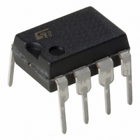
ST7FLITEUS5B6 STMicroelectronics, ST7FLITEUS5B6 Datasheet - Page 93

ST7FLITEUS5B6
Manufacturer Part Number
ST7FLITEUS5B6
Description
MCU 8BIT 1KB FLASH 128KB 8-DIP
Manufacturer
STMicroelectronics
Series
ST7r
Datasheet
1.STEVAL-IFS006V1.pdf
(136 pages)
Specifications of ST7FLITEUS5B6
Core Processor
ST7
Core Size
8-Bit
Speed
8MHz
Peripherals
LVD, POR, PWM, WDT
Number Of I /o
5
Program Memory Size
1KB (1K x 8)
Program Memory Type
FLASH
Ram Size
128 x 8
Voltage - Supply (vcc/vdd)
2.4 V ~ 5.5 V
Data Converters
A/D 5x10b
Oscillator Type
Internal
Operating Temperature
-40°C ~ 85°C
Package / Case
8-DIP (0.300", 7.62mm)
Controller Family/series
ST7
No. Of I/o's
5
Ram Memory Size
128Byte
Cpu Speed
8MHz
No. Of Timers
2
Rohs Compliant
Yes
For Use With
497-6403 - BOARD EVAL 8BIT MICRO + TDE1708497-6407 - BOARD EVAL FOR VACUUM CLEANER497-5861 - EVAL BRD POWER MOSFET/8PIN MCU497-5858 - EVAL BOARD PLAYBACK ST7FLITE497-5515 - EVAL BOARD PHASE CTRL DIMMER497-5049 - KIT STARTER RAISONANCE ST7FLITE497-5046 - KIT TOOL FOR ST7/UPSD/STR7 MCU
Lead Free Status / RoHS Status
Lead free / RoHS Compliant
Eeprom Size
-
Connectivity
-
Other names
497-5636-5
Available stocks
Company
Part Number
Manufacturer
Quantity
Price
Company:
Part Number:
ST7FLITEUS5B6
Manufacturer:
STMicroelectronics
Quantity:
8
ST7LITEUS2, ST7LITEUS5
12.1.5
12.2
Pin input voltage
The input voltage measurement on a pin of the device is described in
Figure 38. Pin input voltage
Absolute maximum ratings
Stresses above those listed as “absolute maximum ratings” may cause permanent damage
to the device. This is a stress rating only and functional operation of the device under these
conditions is not implied. Exposure to maximum rating conditions for extended periods may
affect device reliability.
1. Directly connecting the I/O pins to V
change of the I/O configuration occurs (for example, due to a corrupted program counter).
To guarantee safe operation, this connection has to be done through a pull-up or pull-down
resistor (typical: 10 kΩ for I/Os). Unused I/O pins must be tied in the same way to V
V
Table 43.
1. I
SS
cannot be respected, the injection current must be limited externally to the I
injection is induced by V
INJ(PIN)
according to their reset configuration.
V
V
V
Symbol
ESD(HBM)
DD
ESD(MM)
V
- V
IN
must never be exceeded. This is implicitly insured if V
SS
Voltage characteristics
Supply voltage
Input voltage on any pin
Electrostatic discharge voltage (Human Body
Model)
Electrostatic discharge voltage (Machine
Model)
IN
>V
DD
while a negative injection is induced by V
Ratings
V
DD
IN
(1)
or V
SS
could damage the device if an unexpected
ST7 PIN
IN
maximum is respected. If V
IN
V
INJ(PIN)
<V
Maximum value
SS
Electrical characteristics
SS
-0.3 to V
.
see
see
value. A positive
Figure
7.0
Section 12.7.2
Section 12.7.2
DD
IN
38.
+0.3
maximum
DD
Unit
93/136
V
or


