ST7FLITEUS5B6 STMicroelectronics, ST7FLITEUS5B6 Datasheet - Page 73

ST7FLITEUS5B6
Manufacturer Part Number
ST7FLITEUS5B6
Description
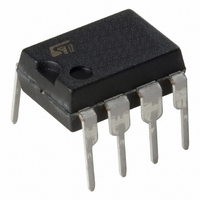
MCU 8BIT 1KB FLASH 128KB 8-DIP
Manufacturer
STMicroelectronics
Series
ST7r
Datasheet
1.STEVAL-IFS006V1.pdf
(136 pages)
Specifications of ST7FLITEUS5B6
Core Processor
ST7
Core Size
8-Bit
Speed
8MHz
Peripherals
LVD, POR, PWM, WDT
Number Of I /o
5
Program Memory Size
1KB (1K x 8)
Program Memory Type
FLASH
Ram Size
128 x 8
Voltage - Supply (vcc/vdd)
2.4 V ~ 5.5 V
Data Converters
A/D 5x10b
Oscillator Type
Internal
Operating Temperature
-40°C ~ 85°C
Package / Case
8-DIP (0.300", 7.62mm)
Controller Family/series
ST7
No. Of I/o's
5
Ram Memory Size
128Byte
Cpu Speed
8MHz
No. Of Timers
2
Rohs Compliant
Yes
For Use With
497-6403 - BOARD EVAL 8BIT MICRO + TDE1708497-6407 - BOARD EVAL FOR VACUUM CLEANER497-5861 - EVAL BRD POWER MOSFET/8PIN MCU497-5858 - EVAL BOARD PLAYBACK ST7FLITE497-5515 - EVAL BOARD PHASE CTRL DIMMER497-5049 - KIT STARTER RAISONANCE ST7FLITE497-5046 - KIT TOOL FOR ST7/UPSD/STR7 MCU
Lead Free Status / RoHS Status
Lead free / RoHS Compliant
Eeprom Size
-
Connectivity
-
Other names
497-5636-5
Available stocks
Company
Part Number
Manufacturer
Quantity
Price
Company:
Part Number:
ST7FLITEUS5B6
Manufacturer:
STMicroelectronics
Quantity:
8
ST7LITEUS2, ST7LITEUS5
Note:
Caution:
10.2.4
Figure 35. PWM signal example
Output compare mode
To use this function, the OE bit must be 0, otherwise the compare is done with the shadow
register instead of the DCRx register. Software must then write a 12-bit value in the DCR0H
and DCR0L registers. This value will be loaded immediately (without waiting for an OVF
event).
The DCR0H must be written first, the output compare function starts only when the DCR0L
value is written.
When the 12-bit upcounter (CNTR) reaches the value stored in the DCR0H and DCR0L
registers, the CMPF0 bit in the PWM0CSR register is set and an interrupt request is
generated if the CMPIE bit is set.
The output compare function is only available for DCRx values other than 0 (reset value).
At each OVF event, the DCRx value is written in a shadow register, even if the DCR0L value
has not yet been written (in this case, the shadow register will contain the new DCR0H value
and the old DCR0L value), then:
Low power modes
Table 27.
–
–
If OE=1 (PWM mode): the compare is done between the timer counter and the
shadow register (and not DCRx)
If OE=0 (OCMP mode): the compare is done between the timer counter and
DCRx. There is no PWM signal.
The compare between DCRx or the shadow register and the timer counter is
locked until DCR0L is written.
Active-halt
Description of low power modes
Mode
DCR0=FFEh
Slow
Wait
Halt
COUNTER
f
COUNTER
FFDh
FFEh
AT timer halted except if CK0=1, CK1=0 and OVFIE=1
ATR= FFDh
FFFh
The input frequency is divided by 32
FFDh
No effect on AT timer
FFEh
AT timer halted
Description
FFFh
FFDh
On-chip peripherals
FFEh
t
73/136


