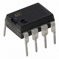
ST7FLITEUS5B6 STMicroelectronics, ST7FLITEUS5B6 Datasheet - Page 80

ST7FLITEUS5B6
Manufacturer Part Number
ST7FLITEUS5B6
Description
MCU 8BIT 1KB FLASH 128KB 8-DIP
Manufacturer
STMicroelectronics
Series
ST7r
Datasheet
1.STEVAL-IFS006V1.pdf
(136 pages)
Specifications of ST7FLITEUS5B6
Core Processor
ST7
Core Size
8-Bit
Speed
8MHz
Peripherals
LVD, POR, PWM, WDT
Number Of I /o
5
Program Memory Size
1KB (1K x 8)
Program Memory Type
FLASH
Ram Size
128 x 8
Voltage - Supply (vcc/vdd)
2.4 V ~ 5.5 V
Data Converters
A/D 5x10b
Oscillator Type
Internal
Operating Temperature
-40°C ~ 85°C
Package / Case
8-DIP (0.300", 7.62mm)
Controller Family/series
ST7
No. Of I/o's
5
Ram Memory Size
128Byte
Cpu Speed
8MHz
No. Of Timers
2
Rohs Compliant
Yes
For Use With
497-6403 - BOARD EVAL 8BIT MICRO + TDE1708497-6407 - BOARD EVAL FOR VACUUM CLEANER497-5861 - EVAL BRD POWER MOSFET/8PIN MCU497-5858 - EVAL BOARD PLAYBACK ST7FLITE497-5515 - EVAL BOARD PHASE CTRL DIMMER497-5049 - KIT STARTER RAISONANCE ST7FLITE497-5046 - KIT TOOL FOR ST7/UPSD/STR7 MCU
Lead Free Status / RoHS Status
Lead free / RoHS Compliant
Eeprom Size
-
Connectivity
-
Other names
497-5636-5
Available stocks
Company
Part Number
Manufacturer
Quantity
Price
Company:
Part Number:
ST7FLITEUS5B6
Manufacturer:
STMicroelectronics
Quantity:
8
On-chip peripherals
80/136
Figure 36. ADC block diagram
Digital A/D conversion result
The conversion is monotonic, meaning that the result never decreases if the analog input
does not and never increases if the analog input does not.
If the input voltage (V
conversion result is FFh in the ADCDRH register and 03h in the ADCDRL register (without
overflow indication).
If the input voltage (V
conversion result in the ADCDRH and ADCDRL registers is 00 00h.
The A/D converter is linear and the digital result of the conversion is stored in the ADCDRH
and ADCDRL registers. The accuracy of the conversion is described in the Electrical
Characteristics Section.
R
is too high, this will result in a loss of accuracy due to leakage and sampling not being
completed in the alloted time.
A/D conversion phases
The A/D conversion is based on two conversion phases:
●
●
AIN
AIN0
AIN1
AINx
Sample capacitor loading [duration: t
During this phase, the V
sample capacitor.
A/D conversion [duration: t
During this phase, the A/D conversion is computed (8 successive approximations
is the maximum recommended impedance for an analog input signal. If the impedance
f
CPU
ANALOG
DIV 2
MUX
EOC SPEED ADON
AIN
AIN
3
ADCDRH
) is greater than V
) is lower than V
0
1
AIN
HOLD
DIV 4
input voltage to be measured is loaded into the C
0
R
ADCDRL
ADC
D9
]
0
CH2
D8
SSA
SAMPLE
SLOW
DDA
bit
1
0
CH1
D7
HOLD CONTROL
(low-level voltage reference) then the
(high-level voltage reference) then the
0
CH0
D6
]
0
f
C
ADC
ADC
D5
ADCCSR
0
D4
0
ANALOG TO DIGITAL
D3
SLOW
CONVERTER
ST7LITEUS2, ST7LITEUS5
D2
0
D1
D0
ADC


