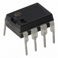
ST7FLITEUS5B6 STMicroelectronics, ST7FLITEUS5B6 Datasheet - Page 115

ST7FLITEUS5B6
Manufacturer Part Number
ST7FLITEUS5B6
Description
MCU 8BIT 1KB FLASH 128KB 8-DIP
Manufacturer
STMicroelectronics
Series
ST7r
Datasheet
1.STEVAL-IFS006V1.pdf
(136 pages)
Specifications of ST7FLITEUS5B6
Core Processor
ST7
Core Size
8-Bit
Speed
8MHz
Peripherals
LVD, POR, PWM, WDT
Number Of I /o
5
Program Memory Size
1KB (1K x 8)
Program Memory Type
FLASH
Ram Size
128 x 8
Voltage - Supply (vcc/vdd)
2.4 V ~ 5.5 V
Data Converters
A/D 5x10b
Oscillator Type
Internal
Operating Temperature
-40°C ~ 85°C
Package / Case
8-DIP (0.300", 7.62mm)
Controller Family/series
ST7
No. Of I/o's
5
Ram Memory Size
128Byte
Cpu Speed
8MHz
No. Of Timers
2
Rohs Compliant
Yes
For Use With
497-6403 - BOARD EVAL 8BIT MICRO + TDE1708497-6407 - BOARD EVAL FOR VACUUM CLEANER497-5861 - EVAL BRD POWER MOSFET/8PIN MCU497-5858 - EVAL BOARD PLAYBACK ST7FLITE497-5515 - EVAL BOARD PHASE CTRL DIMMER497-5049 - KIT STARTER RAISONANCE ST7FLITE497-5046 - KIT TOOL FOR ST7/UPSD/STR7 MCU
Lead Free Status / RoHS Status
Lead free / RoHS Compliant
Eeprom Size
-
Connectivity
-
Other names
497-5636-5
Available stocks
Company
Part Number
Manufacturer
Quantity
Price
Company:
Part Number:
ST7FLITEUS5B6
Manufacturer:
STMicroelectronics
Quantity:
8
ST7LITEUS2, ST7LITEUS5
12.10
Figure 62. RESET pin protection when LVD is disabled
ADC characteristics
Subject to general operating condition for V
Table 66.
1. Unless otherwise specified, typical data are based on T
2. The maximum ADC clock frequency allowed within V
3. When V
4. Any added external serial resistor will downgrade the ADC accuracy (especially for resistance greater than
5. The stabilization time of the A/D converter is masked by the first t
Symbol
C
t
R
f
V
t
STAB
ADC
ADC
design guidelines and are not tested.
10k
enable is then always valid.
ADC
AIN
AIN
Required
Ω
EXTERNAL
CIRCUIT
). Data based on characterization results, not tested in production.
RESET
USER
ADC clock frequency
Conversion voltage range
External input resistor
Internal sample and hold
capacitor
Stabilization time after ADC
enable
Conversion time
(Sample+Hold)
- Sample capacitor loading
time
- Hold conversion time
DDA
10-bit ADC characteristics
and V
Parameter
SSA
0.01μF
pins are not available on the pinout, the ADC refers to V
(2)
(3)
V
V
f
2.7 V ≤ V
f
2.4 V ≤ V
f
f
f
ADC
ADC
ADC
CPU
ADC
V
DD
DD
DD
R
=4 MHz
=2 MHz
=1 MHz
=8 MHz,
=4 MHz
= 5 V, f
= 3.3 V,
ON
Conditions
DD
Filter
DD
DD
DD
, f
GENERATOR
ADC
A
OSC
≤5.5 V,
≤2.7 V,
= 2.4 to 2.7 V operating range is 1 MHz.
=25°C and V
PULSE
=4 MHz
, and T
LOAD
A
DD
. The first conversion after the
unless otherwise specified.
-V
V
Min
SSA
SS
=5 V. They are given only as
Electrical characteristics
DD
WATCHDOG
Typ
and V
ILLEGAL OPCODE
0
3.5
10
3
4
(5)
(1)
INTERNAL
RESET
SS.
ST7XXX
TBD
V
10
Max
8
7
DDA
4
(4)
(4)
(4)
(4)
5)
115/136
1/f
MHz
Unit
kΩ
pF
μs
V
ADC


