ST7FLITEUS5B6 STMicroelectronics, ST7FLITEUS5B6 Datasheet - Page 77

ST7FLITEUS5B6
Manufacturer Part Number
ST7FLITEUS5B6
Description
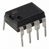
MCU 8BIT 1KB FLASH 128KB 8-DIP
Manufacturer
STMicroelectronics
Series
ST7r
Datasheet
1.STEVAL-IFS006V1.pdf
(136 pages)
Specifications of ST7FLITEUS5B6
Core Processor
ST7
Core Size
8-Bit
Speed
8MHz
Peripherals
LVD, POR, PWM, WDT
Number Of I /o
5
Program Memory Size
1KB (1K x 8)
Program Memory Type
FLASH
Ram Size
128 x 8
Voltage - Supply (vcc/vdd)
2.4 V ~ 5.5 V
Data Converters
A/D 5x10b
Oscillator Type
Internal
Operating Temperature
-40°C ~ 85°C
Package / Case
8-DIP (0.300", 7.62mm)
Controller Family/series
ST7
No. Of I/o's
5
Ram Memory Size
128Byte
Cpu Speed
8MHz
No. Of Timers
2
Rohs Compliant
Yes
For Use With
497-6403 - BOARD EVAL 8BIT MICRO + TDE1708497-6407 - BOARD EVAL FOR VACUUM CLEANER497-5861 - EVAL BRD POWER MOSFET/8PIN MCU497-5858 - EVAL BOARD PLAYBACK ST7FLITE497-5515 - EVAL BOARD PHASE CTRL DIMMER497-5049 - KIT STARTER RAISONANCE ST7FLITE497-5046 - KIT TOOL FOR ST7/UPSD/STR7 MCU
Lead Free Status / RoHS Status
Lead free / RoHS Compliant
Eeprom Size
-
Connectivity
-
Other names
497-5636-5
Available stocks
Company
Part Number
Manufacturer
Quantity
Price
Company:
Part Number:
ST7FLITEUS5B6
Manufacturer:
STMicroelectronics
Quantity:
8
ST7LITEUS2, ST7LITEUS5
PWM0 control/status register (PWM0CSR)
Reset value: 0000 0000 (00h)
PWM output control register (PWMCR)
Reset value: 0000 0000 (00h)
Table 30.
Address
(Hex.)
0D
0E
0F
10
7
0
7
0
Bits 7:1 Reserved, must be kept cleared.
Bit 7:2 Reserved, must be kept cleared.
ATCSR
Reset value
CNTRH
Reset value
CNTRL
Reset value
ATRH
Reset value
Bit 1 OP0 PWM0 output polarity.
Bit 0 CMPF0 PWM0 Compare Flag.
Bit 0 OE0 PWM0 Output enable.
Register
Register map and reset values
label
0
This bit is read/write by software and cleared by hardware after a reset. This bit
selects the polarity of the PWM0 signal.
0: The PWM0 signal is not inverted.
1: The PWM0 signal is inverted.
This bit is set by hardware and cleared by software by reading the PWM0CSR
register. It indicates that the upcounter value matches the DCR0 register value.
0: Upcounter value does not match DCR value.
1: Upcounter value matches DCR value.
0
This bit is set and cleared by software.
0: PWM0 output Alternate Function disabled (I/O pin free for general purpose I/O)
1: PWM0 output enabled
CN7
7
0
0
0
0
0
0
CN6
6
0
0
0
0
0
0
Read/Write
Read/Write
CN5
5
0
0
0
0
CN4
CK1
0
0
4
0
0
0
0
ATR11
CN11
CN3
CK0
3
0
0
0
0
0
0
ATR10
CN10
OVF
CN2
2
0
0
0
0
On-chip peripherals
OP0
0
OVFIE
ATR9
CN9
CN1
1
0
0
0
0
CMPF0
CMPIE
OE0
ATR8
CN8
CN0
0
0
77/136
0
0
0
0
0


