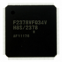
DF2378RVFQ34V Renesas Electronics America, DF2378RVFQ34V Datasheet - Page 703

DF2378RVFQ34V
Manufacturer Part Number
DF2378RVFQ34V
Description
IC H8S MCU FLASH 512K 144LQFP
Manufacturer
Renesas Electronics America
Series
H8® H8S/2300r
Specifications of DF2378RVFQ34V
Core Processor
H8S/2000
Core Size
16-Bit
Speed
34MHz
Connectivity
I²C, IrDA, SCI, SmartCard
Peripherals
DMA, POR, PWM, WDT
Number Of I /o
97
Program Memory Size
512KB (512K x 8)
Program Memory Type
FLASH
Ram Size
32K x 8
Voltage - Supply (vcc/vdd)
3 V ~ 3.6 V
Data Converters
A/D 16x10b; D/A 6x8b
Oscillator Type
Internal
Operating Temperature
-20°C ~ 75°C
Package / Case
144-LQFP
For Use With
YLCDRSK2378 - KIT DEV EVAL H8S/2378 LCDYR0K42378FC000BA - KIT EVAL FOR H8S/2378HS0005KCU11H - EMULATOR E10A-USB H8S(X),SH2(A)EDK2378 - DEV EVAL KIT FOR H8S/2378
Lead Free Status / RoHS Status
Lead free / RoHS Compliant
Eeprom Size
-
Available stocks
Company
Part Number
Manufacturer
Quantity
Price
Company:
Part Number:
DF2378RVFQ34V
Manufacturer:
Renesas Electronics America
Quantity:
10 000
- Current page: 703 of 1208
- Download datasheet (8Mb)
12.3.2
PODRH and PODRL store output data for use in pulse output. A bit that has been set for pulse
output by NDER is read-only and cannot be modified.
PODRH
Bit
7
6
5
4
3
2
1
0
PODRL
Bit
7
6
5
4
3
2
1
0
12.3.3
NDRH, NDRL store the next data for pulse output. The NDR addresses differ depending on
whether pulse output groups have the same output trigger or different output triggers.
Bit Name
POD15
POD14
POD13
POD12
POD11
POD10
POD9
POD8
Bit Name
POD7
POD6
POD5
POD4
POD3
POD2
POD1
POD0
Output Data Registers H, L (PODRH, PODRL)
Next Data Registers H, L (NDRH, NDRL)
Initial Value
0
0
0
0
0
0
0
0
Initial Value
0
0
0
0
0
0
0
0
R/W
R/W
R/W
R/W
R/W
R/W
R/W
R/W
R/W
R/W
R/W
R/W
R/W
R/W
R/W
R/W
R/W
R/W
Description
Output Data Register 15 to 8
For bits which have been set to pulse output by
NDERH, the output trigger transfers NDRH values
to this register during PPG operation. While
NDERH is set to 1, the CPU cannot write to this
register. While NDERH is cleared, the initial output
value of the pulse can be set.
Description
Output Data Register 7 to 0
For bits which have been set to pulse output by
NDERL, the output trigger transfers NDRL values
to this register during PPG operation. While
NDERL is set to 1, the CPU cannot write to this
register. While NDERL is cleared, the initial output
value of the pulse can be set.
Section 12 Programmable Pulse Generator (PPG)
Rev.7.00 Mar. 18, 2009 page 635 of 1136
REJ09B0109-0700
Related parts for DF2378RVFQ34V
Image
Part Number
Description
Manufacturer
Datasheet
Request
R

Part Number:
Description:
KIT STARTER FOR M16C/29
Manufacturer:
Renesas Electronics America
Datasheet:

Part Number:
Description:
KIT STARTER FOR R8C/2D
Manufacturer:
Renesas Electronics America
Datasheet:

Part Number:
Description:
R0K33062P STARTER KIT
Manufacturer:
Renesas Electronics America
Datasheet:

Part Number:
Description:
KIT STARTER FOR R8C/23 E8A
Manufacturer:
Renesas Electronics America
Datasheet:

Part Number:
Description:
KIT STARTER FOR R8C/25
Manufacturer:
Renesas Electronics America
Datasheet:

Part Number:
Description:
KIT STARTER H8S2456 SHARPE DSPLY
Manufacturer:
Renesas Electronics America
Datasheet:

Part Number:
Description:
KIT STARTER FOR R8C38C
Manufacturer:
Renesas Electronics America
Datasheet:

Part Number:
Description:
KIT STARTER FOR R8C35C
Manufacturer:
Renesas Electronics America
Datasheet:

Part Number:
Description:
KIT STARTER FOR R8CL3AC+LCD APPS
Manufacturer:
Renesas Electronics America
Datasheet:

Part Number:
Description:
KIT STARTER FOR RX610
Manufacturer:
Renesas Electronics America
Datasheet:

Part Number:
Description:
KIT STARTER FOR R32C/118
Manufacturer:
Renesas Electronics America
Datasheet:

Part Number:
Description:
KIT DEV RSK-R8C/26-29
Manufacturer:
Renesas Electronics America
Datasheet:

Part Number:
Description:
KIT STARTER FOR SH7124
Manufacturer:
Renesas Electronics America
Datasheet:

Part Number:
Description:
KIT STARTER FOR H8SX/1622
Manufacturer:
Renesas Electronics America
Datasheet:

Part Number:
Description:
KIT DEV FOR SH7203
Manufacturer:
Renesas Electronics America
Datasheet:


