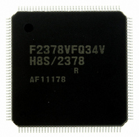
DF2378RVFQ34V Renesas Electronics America, DF2378RVFQ34V Datasheet - Page 719

DF2378RVFQ34V
Manufacturer Part Number
DF2378RVFQ34V
Description
IC H8S MCU FLASH 512K 144LQFP
Manufacturer
Renesas Electronics America
Series
H8® H8S/2300r
Specifications of DF2378RVFQ34V
Core Processor
H8S/2000
Core Size
16-Bit
Speed
34MHz
Connectivity
I²C, IrDA, SCI, SmartCard
Peripherals
DMA, POR, PWM, WDT
Number Of I /o
97
Program Memory Size
512KB (512K x 8)
Program Memory Type
FLASH
Ram Size
32K x 8
Voltage - Supply (vcc/vdd)
3 V ~ 3.6 V
Data Converters
A/D 16x10b; D/A 6x8b
Oscillator Type
Internal
Operating Temperature
-20°C ~ 75°C
Package / Case
144-LQFP
For Use With
YLCDRSK2378 - KIT DEV EVAL H8S/2378 LCDYR0K42378FC000BA - KIT EVAL FOR H8S/2378HS0005KCU11H - EMULATOR E10A-USB H8S(X),SH2(A)EDK2378 - DEV EVAL KIT FOR H8S/2378
Lead Free Status / RoHS Status
Lead free / RoHS Compliant
Eeprom Size
-
Available stocks
Company
Part Number
Manufacturer
Quantity
Price
Company:
Part Number:
DF2378RVFQ34V
Manufacturer:
Renesas Electronics America
Quantity:
10 000
- Current page: 719 of 1208
- Download datasheet (8Mb)
12.4.8
Pulse output can be triggered by TPU input capture as well as by compare match. If TGRA
functions as an input capture register in the TPU channel selected by PCR, pulse output will be
triggered by the input capture signal.
Figure 12.11 shows the timing of this output.
12.5
12.5.1
PPG operation can be disabled or enabled using the module stop control register. The initial value
is for PPG operation to be halted. Register access is enabled by clearing module stop mode. For
details, refer to section 24, Power-Down Modes.
12.5.2
Pins PO0 to PO15 are also used for other peripheral functions such as the TPU. When output by
another peripheral function is enabled, the corresponding pins cannot be used for pulse output.
Note, however, that data transfer from NDR bits to PODR bits takes place, regardless of the usage
of the pins.
Pin functions should be changed only under conditions in which the output trigger event will not
occur.
φ
TIOC pin
Input capture
signal
NDR
PODR
PO
Pulse Output Triggered by Input Capture
Usage Notes
Module Stop Mode Setting
Operation of Pulse Output Pins
Figure 12.11 Pulse Output Triggered by Input Capture (Example)
M
M
Section 12 Programmable Pulse Generator (PPG)
N
Rev.7.00 Mar. 18, 2009 page 651 of 1136
N
N
REJ09B0109-0700
Related parts for DF2378RVFQ34V
Image
Part Number
Description
Manufacturer
Datasheet
Request
R

Part Number:
Description:
KIT STARTER FOR M16C/29
Manufacturer:
Renesas Electronics America
Datasheet:

Part Number:
Description:
KIT STARTER FOR R8C/2D
Manufacturer:
Renesas Electronics America
Datasheet:

Part Number:
Description:
R0K33062P STARTER KIT
Manufacturer:
Renesas Electronics America
Datasheet:

Part Number:
Description:
KIT STARTER FOR R8C/23 E8A
Manufacturer:
Renesas Electronics America
Datasheet:

Part Number:
Description:
KIT STARTER FOR R8C/25
Manufacturer:
Renesas Electronics America
Datasheet:

Part Number:
Description:
KIT STARTER H8S2456 SHARPE DSPLY
Manufacturer:
Renesas Electronics America
Datasheet:

Part Number:
Description:
KIT STARTER FOR R8C38C
Manufacturer:
Renesas Electronics America
Datasheet:

Part Number:
Description:
KIT STARTER FOR R8C35C
Manufacturer:
Renesas Electronics America
Datasheet:

Part Number:
Description:
KIT STARTER FOR R8CL3AC+LCD APPS
Manufacturer:
Renesas Electronics America
Datasheet:

Part Number:
Description:
KIT STARTER FOR RX610
Manufacturer:
Renesas Electronics America
Datasheet:

Part Number:
Description:
KIT STARTER FOR R32C/118
Manufacturer:
Renesas Electronics America
Datasheet:

Part Number:
Description:
KIT DEV RSK-R8C/26-29
Manufacturer:
Renesas Electronics America
Datasheet:

Part Number:
Description:
KIT STARTER FOR SH7124
Manufacturer:
Renesas Electronics America
Datasheet:

Part Number:
Description:
KIT STARTER FOR H8SX/1622
Manufacturer:
Renesas Electronics America
Datasheet:

Part Number:
Description:
KIT DEV FOR SH7203
Manufacturer:
Renesas Electronics America
Datasheet:


