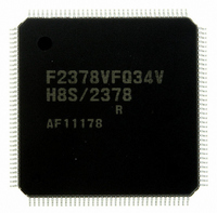
DF2378RVFQ34V Renesas Electronics America, DF2378RVFQ34V Datasheet - Page 959

DF2378RVFQ34V
Manufacturer Part Number
DF2378RVFQ34V
Description
IC H8S MCU FLASH 512K 144LQFP
Manufacturer
Renesas Electronics America
Series
H8® H8S/2300r
Specifications of DF2378RVFQ34V
Core Processor
H8S/2000
Core Size
16-Bit
Speed
34MHz
Connectivity
I²C, IrDA, SCI, SmartCard
Peripherals
DMA, POR, PWM, WDT
Number Of I /o
97
Program Memory Size
512KB (512K x 8)
Program Memory Type
FLASH
Ram Size
32K x 8
Voltage - Supply (vcc/vdd)
3 V ~ 3.6 V
Data Converters
A/D 16x10b; D/A 6x8b
Oscillator Type
Internal
Operating Temperature
-20°C ~ 75°C
Package / Case
144-LQFP
For Use With
YLCDRSK2378 - KIT DEV EVAL H8S/2378 LCDYR0K42378FC000BA - KIT EVAL FOR H8S/2378HS0005KCU11H - EMULATOR E10A-USB H8S(X),SH2(A)EDK2378 - DEV EVAL KIT FOR H8S/2378
Lead Free Status / RoHS Status
Lead free / RoHS Compliant
Eeprom Size
-
Available stocks
Company
Part Number
Manufacturer
Quantity
Price
Company:
Part Number:
DF2378RVFQ34V
Manufacturer:
Renesas Electronics America
Quantity:
10 000
- Current page: 959 of 1208
- Download datasheet (8Mb)
21.4
When the pin is set in on-board programming mode and the reset start is executed, the on-board
programming state that can program/erase the on-chip flash memory is entered. On-board
programming mode has three operating modes: user programming mode, user boot mode, and
boot mode.
For details of the pin setting for entering each mode, see table 21.5. User programming mode can
be used by setting the control bit (FLSHE) by software. For details of the state transition of each
mode for flash memory, see figure 21.2.
Table 21.5 Setting On-Board Programming Mode
Mode Setting
Boot mode
User boot mode
21.4.1
Boot mode executes programming/erasing user MAT and user boot MAT by means of the control
command and program data transmitted from the host using the on-chip SCI. The tool for
transmitting the control command and program data must be prepared in the host. The SCI
communication mode is set to asynchronous mode. When reset start is executed after this LSI’s
pin is set in boot mode, the boot program in the microcomputer is initiated. After the SCI bit rate
is automatically adjusted, the communication with the host is executed by means of the control
command method.
The system configuration diagram in boot mode is shown in figure 21.6. For details on the pin
setting in boot mode, see table 21.5. The NMI and other interrupts are ignored in boot mode.
However, the NMI and other interrupts should be disabled in the user system.
On-Board Programming Mode
Boot Mode
Advanced mode
Advanced mode
Section 21 Flash Memory (0.18-μm F-ZTAT Version)
1
MD2
0
Rev.7.00 Mar. 18, 2009 page 891 of 1136
MD1
1
0
REJ09B0109-0700
MD0
1
1
Related parts for DF2378RVFQ34V
Image
Part Number
Description
Manufacturer
Datasheet
Request
R

Part Number:
Description:
KIT STARTER FOR M16C/29
Manufacturer:
Renesas Electronics America
Datasheet:

Part Number:
Description:
KIT STARTER FOR R8C/2D
Manufacturer:
Renesas Electronics America
Datasheet:

Part Number:
Description:
R0K33062P STARTER KIT
Manufacturer:
Renesas Electronics America
Datasheet:

Part Number:
Description:
KIT STARTER FOR R8C/23 E8A
Manufacturer:
Renesas Electronics America
Datasheet:

Part Number:
Description:
KIT STARTER FOR R8C/25
Manufacturer:
Renesas Electronics America
Datasheet:

Part Number:
Description:
KIT STARTER H8S2456 SHARPE DSPLY
Manufacturer:
Renesas Electronics America
Datasheet:

Part Number:
Description:
KIT STARTER FOR R8C38C
Manufacturer:
Renesas Electronics America
Datasheet:

Part Number:
Description:
KIT STARTER FOR R8C35C
Manufacturer:
Renesas Electronics America
Datasheet:

Part Number:
Description:
KIT STARTER FOR R8CL3AC+LCD APPS
Manufacturer:
Renesas Electronics America
Datasheet:

Part Number:
Description:
KIT STARTER FOR RX610
Manufacturer:
Renesas Electronics America
Datasheet:

Part Number:
Description:
KIT STARTER FOR R32C/118
Manufacturer:
Renesas Electronics America
Datasheet:

Part Number:
Description:
KIT DEV RSK-R8C/26-29
Manufacturer:
Renesas Electronics America
Datasheet:

Part Number:
Description:
KIT STARTER FOR SH7124
Manufacturer:
Renesas Electronics America
Datasheet:

Part Number:
Description:
KIT STARTER FOR H8SX/1622
Manufacturer:
Renesas Electronics America
Datasheet:

Part Number:
Description:
KIT DEV FOR SH7203
Manufacturer:
Renesas Electronics America
Datasheet:


