DF2378RVFQ34V Renesas Electronics America, DF2378RVFQ34V Datasheet - Page 968
DF2378RVFQ34V
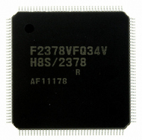
Manufacturer Part Number
DF2378RVFQ34V
Description
IC H8S MCU FLASH 512K 144LQFP
Manufacturer
Renesas Electronics America
Series
H8® H8S/2300r
Specifications of DF2378RVFQ34V
Core Processor
H8S/2000
Core Size
16-Bit
Speed
34MHz
Connectivity
I²C, IrDA, SCI, SmartCard
Peripherals
DMA, POR, PWM, WDT
Number Of I /o
97
Program Memory Size
512KB (512K x 8)
Program Memory Type
FLASH
Ram Size
32K x 8
Voltage - Supply (vcc/vdd)
3 V ~ 3.6 V
Data Converters
A/D 16x10b; D/A 6x8b
Oscillator Type
Internal
Operating Temperature
-20°C ~ 75°C
Package / Case
144-LQFP
For Use With
YLCDRSK2378 - KIT DEV EVAL H8S/2378 LCDYR0K42378FC000BA - KIT EVAL FOR H8S/2378HS0005KCU11H - EMULATOR E10A-USB H8S(X),SH2(A)EDK2378 - DEV EVAL KIT FOR H8S/2378
Lead Free Status / RoHS Status
Lead free / RoHS Compliant
Eeprom Size
-
Available stocks
Company
Part Number
Manufacturer
Quantity
Price
Company:

Part Number:
DF2378RVFQ34V
Manufacturer:
Renesas Electronics America
Quantity:
10 000


Section 21 Flash Memory (0.18-μm F-ZTAT Version)
6. The FPEFEQ and FUBRA parameters are set for initialization.
Note: * 8 to 35 MHz in H8S/2378.
7. Initialization
Rev.7.00 Mar. 18, 2009 page 900 of 1136
REJ09B0109-0700
⎯ If the value of the DPFR parameter is different from before downloading, check the SS bit
⎯ The current frequency of the CPU clock is set to the FPEFEQ parameter (general register
⎯ Set the user branch destination address as the FUBRA parameter (general register ER1)
When a programming program is downloaded, the initialization program is also downloaded to
the on-chip RAM. There is an entry point of the initialization program in the area from the start
address specified by FTDAR + 32 bytes of the on-chip RAM. The subroutine is called and
initialization is executed by using the following steps.
MOV.L
JSR
NOP
⎯ The general registers other than ER0, ER1 are held in the initialization program.
⎯ R0L is a return value of the FPFR parameter.
⎯ Since the stack area is used in the initialization program, a stack area of a maximum 128
(bit 2) and the FK bit (bit 1) in the DPFR parameter to ensure that the download program
selection and FKEY setting were normal, respectively.
ER0).
The allowable setting range for the FPEFEQ parameter is 8 MHz to 34 MHz * . When the
frequency is set to out of this range, an error is returned to the FPFR parameter of the
initialization program and initialization is not performed. For details on the frequency
setting, see the description in 21.3.2 (2) (a), Flash programming/erasing frequency
parameter (FPEFEQ: general register ER0 of CPU).
and the user branch enable bits (FUBE15 to FUBE0) as the FPEFEQ parameter (general
register ER0). Set FUBRA and FUBE15 to FUBE0 to 0 if the user branch function is not
required.
Do use programmable user MAT as the user branch destination. Also, do not use an area
containing a downloaded internal program as the user branch destination. After user branch
processing completes, use the RTS instruction to return to programming processing.
For details, see the descriptions in 21.3.2 (2) (a), Flash programming/erasing frequency
parameter (FPEFEQ: general register ER0 of CPU), and 21.3.2 (2) (b), Flash user branch
address setting parameter (FUBRA: general register ER1 of CPU).
bytes must be allocated in RAM.
DLTOP+32,ER2;
@ER2;
Set entry address to ER2
Call initialization routine
Related parts for DF2378RVFQ34V
Image
Part Number
Description
Manufacturer
Datasheet
Request
R

Part Number:
Description:
KIT STARTER FOR M16C/29
Manufacturer:
Renesas Electronics America
Datasheet:

Part Number:
Description:
KIT STARTER FOR R8C/2D
Manufacturer:
Renesas Electronics America
Datasheet:

Part Number:
Description:
R0K33062P STARTER KIT
Manufacturer:
Renesas Electronics America
Datasheet:

Part Number:
Description:
KIT STARTER FOR R8C/23 E8A
Manufacturer:
Renesas Electronics America
Datasheet:

Part Number:
Description:
KIT STARTER FOR R8C/25
Manufacturer:
Renesas Electronics America
Datasheet:

Part Number:
Description:
KIT STARTER H8S2456 SHARPE DSPLY
Manufacturer:
Renesas Electronics America
Datasheet:

Part Number:
Description:
KIT STARTER FOR R8C38C
Manufacturer:
Renesas Electronics America
Datasheet:

Part Number:
Description:
KIT STARTER FOR R8C35C
Manufacturer:
Renesas Electronics America
Datasheet:

Part Number:
Description:
KIT STARTER FOR R8CL3AC+LCD APPS
Manufacturer:
Renesas Electronics America
Datasheet:
Part Number:
Description:
KIT STARTER FOR RX610
Manufacturer:
Renesas Electronics America
Datasheet:

Part Number:
Description:
KIT STARTER FOR R32C/118
Manufacturer:
Renesas Electronics America
Datasheet:

Part Number:
Description:
KIT DEV RSK-R8C/26-29
Manufacturer:
Renesas Electronics America
Datasheet:

Part Number:
Description:
KIT STARTER FOR SH7124
Manufacturer:
Renesas Electronics America
Datasheet:

Part Number:
Description:
KIT STARTER FOR H8SX/1622
Manufacturer:
Renesas Electronics America
Datasheet:

Part Number:
Description:
KIT DEV FOR SH7203
Manufacturer:
Renesas Electronics America
Datasheet: