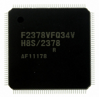
DF2378RVFQ34V Renesas Electronics America, DF2378RVFQ34V Datasheet - Page 818

DF2378RVFQ34V
Manufacturer Part Number
DF2378RVFQ34V
Description
IC H8S MCU FLASH 512K 144LQFP
Manufacturer
Renesas Electronics America
Series
H8® H8S/2300r
Specifications of DF2378RVFQ34V
Core Processor
H8S/2000
Core Size
16-Bit
Speed
34MHz
Connectivity
I²C, IrDA, SCI, SmartCard
Peripherals
DMA, POR, PWM, WDT
Number Of I /o
97
Program Memory Size
512KB (512K x 8)
Program Memory Type
FLASH
Ram Size
32K x 8
Voltage - Supply (vcc/vdd)
3 V ~ 3.6 V
Data Converters
A/D 16x10b; D/A 6x8b
Oscillator Type
Internal
Operating Temperature
-20°C ~ 75°C
Package / Case
144-LQFP
For Use With
YLCDRSK2378 - KIT DEV EVAL H8S/2378 LCDYR0K42378FC000BA - KIT EVAL FOR H8S/2378HS0005KCU11H - EMULATOR E10A-USB H8S(X),SH2(A)EDK2378 - DEV EVAL KIT FOR H8S/2378
Lead Free Status / RoHS Status
Lead free / RoHS Compliant
Eeprom Size
-
Available stocks
Company
Part Number
Manufacturer
Quantity
Price
Company:
Part Number:
DF2378RVFQ34V
Manufacturer:
Renesas Electronics America
Quantity:
10 000
- Current page: 818 of 1208
- Download datasheet (8Mb)
Section 15 Serial Communication Interface (SCI, IrDA)
As in the above sample start character, with the direct convention type, the logic 1 level
corresponds to state Z and the logic 0 level to state A, and transfer is performed in LSB-first order.
The start character data above is H'3B. For the direct convention type, clear the SDIR and SINV
bits in SCMR to 0. According to the Smart Card regulations, clear the O/E bit in SMR to 0 to
select even parity mode.
With the inverse convention type, the logic 1 level corresponds to state A and the logic 0 level to
state Z, and transfer is performed in MSB-first order. The start character data above is H'3F. For
the inverse convention type, set the SDIR and SINV bits in SCMR to 1. According to the Smart
Card regulations, even parity mode is the logic 0 level of the parity bit, and corresponds to state Z.
In this LSI, the SINV bit inverts only data bits D7 to D0. Therefore, set the O/E bit in SMR to 1 to
invert the parity bit for both transmission and reception.
15.7.3
Operation in block transfer mode is the same as that in normal Smart Card interface, except for the
following points.
• In reception, though the parity check is performed, no error signal is output even if an error is
• In transmission, a guard time of at least 1 etu is left between the end of the parity bit and the
• In transmission, because retransmission is not performed, the TEND flag is set to 1, 11.5 etu
• As with the normal Smart Card interface, the ERS flag indicates the error signal status, but
15.7.4
Only the internal clock generated by the on-chip baud rate generator is used as transmit/receive
clock in Smart Card interface. In Smart Card interface mode, the SCI operates on a basic clock
with a frequency of 32, 64, 372, or 256 times the bit rate (fixed at 16 times in normal
asynchronous mode) as determined by bits BCP1 and BCP0. In reception, the SCI samples the
Rev.7.00 Mar. 18, 2009 page 750 of 1136
REJ09B0109-0700
detected. However, the PER bit in SSR is set to 1 and must be cleared before receiving the
parity bit of the next frame.
start of the next frame.
after transmission start.
since error signal transfer is not performed, this flag is always cleared to 0.
Block Transfer Mode
Receive Data Sampling Timing and Reception Margin
(Z)
Figure 15.24 Inverse Convention (SDIR = SINV = O/E = 1)
Ds
A
D7
Z
D6
Z
D5
A
D4
A
D3
A
D2
A
D1
A
D0
A
Dp
Z
(Z) State
Related parts for DF2378RVFQ34V
Image
Part Number
Description
Manufacturer
Datasheet
Request
R

Part Number:
Description:
KIT STARTER FOR M16C/29
Manufacturer:
Renesas Electronics America
Datasheet:

Part Number:
Description:
KIT STARTER FOR R8C/2D
Manufacturer:
Renesas Electronics America
Datasheet:

Part Number:
Description:
R0K33062P STARTER KIT
Manufacturer:
Renesas Electronics America
Datasheet:

Part Number:
Description:
KIT STARTER FOR R8C/23 E8A
Manufacturer:
Renesas Electronics America
Datasheet:

Part Number:
Description:
KIT STARTER FOR R8C/25
Manufacturer:
Renesas Electronics America
Datasheet:

Part Number:
Description:
KIT STARTER H8S2456 SHARPE DSPLY
Manufacturer:
Renesas Electronics America
Datasheet:

Part Number:
Description:
KIT STARTER FOR R8C38C
Manufacturer:
Renesas Electronics America
Datasheet:

Part Number:
Description:
KIT STARTER FOR R8C35C
Manufacturer:
Renesas Electronics America
Datasheet:

Part Number:
Description:
KIT STARTER FOR R8CL3AC+LCD APPS
Manufacturer:
Renesas Electronics America
Datasheet:

Part Number:
Description:
KIT STARTER FOR RX610
Manufacturer:
Renesas Electronics America
Datasheet:

Part Number:
Description:
KIT STARTER FOR R32C/118
Manufacturer:
Renesas Electronics America
Datasheet:

Part Number:
Description:
KIT DEV RSK-R8C/26-29
Manufacturer:
Renesas Electronics America
Datasheet:

Part Number:
Description:
KIT STARTER FOR SH7124
Manufacturer:
Renesas Electronics America
Datasheet:

Part Number:
Description:
KIT STARTER FOR H8SX/1622
Manufacturer:
Renesas Electronics America
Datasheet:

Part Number:
Description:
KIT DEV FOR SH7203
Manufacturer:
Renesas Electronics America
Datasheet:


