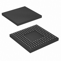
XR17V358IB176-F Exar Corporation, XR17V358IB176-F Datasheet - Page 14

XR17V358IB176-F
Manufacturer Part Number
XR17V358IB176-F
Description
IC UART PCIE OCTAL 176FPBGA
Manufacturer
Exar Corporation
Datasheet
1.XR17V358IB176-F.pdf
(68 pages)
Specifications of XR17V358IB176-F
Number Of Channels
1, UART
Package / Case
176-LFBGA
Features
*
Fifo's
256 Byte
Protocol
RS485
Voltage - Supply
1.2V, 3.3V
With Auto Flow Control
Yes
With Irda Encoder/decoder
Yes
With False Start Bit Detection
Yes
With Modem Control
Yes
Mounting Type
Surface Mount
Data Rate
25 Mbps
Supply Current
120 mA
Maximum Operating Temperature
+ 85 C
Minimum Operating Temperature
- 40 C
Mounting Style
SMD/SMT
Operating Supply Voltage
3.3 V
No. Of Channels
8
Uart Features
Tx/Rx FIFO Counters
Supply Voltage Range
3V To 3.6V
Operating Temperature Range
-40°C To +85°C
Digital Ic Case Style
BGA
No. Of Pins
176
Rohs Compliant
Yes
Lead Free Status / RoHS Status
Lead free / RoHS Compliant
For Use With
1016-1296 - EVAL BOARD FOR XR17V358-E81016-1295 - EVAL BOARD FOR XR17V358-E41016-1293 - EVAL BOARD FOR XR17V358
Lead Free Status / Rohs Status
Lead free / RoHS Compliant
Other names
1016-1294
Available stocks
Company
Part Number
Manufacturer
Quantity
Price
Company:
Part Number:
XR17V358IB176-F
Manufacturer:
EXAR
Quantity:
1 700
Company:
Part Number:
XR17V358IB176-F
Manufacturer:
Exar Corporation
Quantity:
10 000
Part Number:
XR17V358IB176-F
Manufacturer:
EXAR/艾科嘉
Quantity:
20 000
XR17V358
HIGH PERFORMANCE OCTAL PCI EXPRESS UART
N
The V358 provides an interface to an Electrically Erasable Programmable Read Only Memory (EEPROM). The
EEPROM must be a 93C46-like device, with its memory configured as 16-bit words. This interface is provided
in order to program the registers in the PCI Configuration Space of the PCI UART during power-up. The
EEPROM must be organized into address/data pairs. The first word of the pair is the address and the second
word is the data.
Table 3
other Target Addresses are reserved and must not be used.
The second 16-bit word of the address/data pair is the data. The default values are shown in
address/data pairs can be in any order. Only the contents which need to be changed from the Exar defaults
need to be included in the EEPROM.
1.2
OTE
A
O
0x104-
DDRESS
0x113
0x114
FFSET
: EWR=Read/Write from external EEPROM. RWR=Read/Write. RO= Read Only. RWC=Read/Write-Clear.
EEPROM Interface
shows the Target Addresses available for programming into bits 7:0 of the 16-bit address word. All
T
31:0
31:0
ARGET
B
ITS
Table 2
0x00
0x01
0x02
0x03
0x04
0x05
B
A
13:8
7:0
IT
15
14
DDRESS
(
S
)
T
RO
RO
T
YPE
below shows the format of the 16-bit address:
ABLE
T
ABLE
1: PCI L
T
Not implemented or not applicable (return zeros)
VC Offset 0x4
ABLE
Parity Bit - Odd parity over entire address/data pair
If there is a parity error, it will be reported in bit-3 of the REGB register in
the Device Configuration Registers (offset 0x08E).
Final Address
If 1, this will be the last data to be read.
If 0, there will be more data to be read after this.
Reserved - Bits must be ’0’
Target Address - See
lower 8-bits are reserved
3: T
Subsystem Vendor ID
Class Code [23:8]
2: EEPROM A
Class Code [7:0]
OCAL
Subsystem ID
ARGET
Vendor ID
Device ID
D
ATA
B
US
A
DDRESS
C
ONFIGURATION
Table 3
DDRESS
14
D
F
ESCRIPTION
OR
D
B
EEPROM V
EFINITION
IT
0x13A8
0x0358 - No slave
0x4358 - XR17V354 slave present
0x8358 - XR17V358 slave present
0x0200
0x0700
0x0000
0x0000
D
S
EFINITIONS
PACE
ALUES
R
E
EGISTERS
XAR
D
EFAULT
(
HEX OR BINARY
0x8000000FF
R
0x00000000
ESET
Table
REV. 1.0.2
V
ALUE
3. The
)


