XR17V358IB176-F Exar Corporation, XR17V358IB176-F Datasheet - Page 57
XR17V358IB176-F
Manufacturer Part Number
XR17V358IB176-F
Description
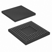
IC UART PCIE OCTAL 176FPBGA
Manufacturer
Exar Corporation
Datasheet
1.XR17V358IB176-F.pdf
(68 pages)
Specifications of XR17V358IB176-F
Number Of Channels
1, UART
Package / Case
176-LFBGA
Features
*
Fifo's
256 Byte
Protocol
RS485
Voltage - Supply
1.2V, 3.3V
With Auto Flow Control
Yes
With Irda Encoder/decoder
Yes
With False Start Bit Detection
Yes
With Modem Control
Yes
Mounting Type
Surface Mount
Data Rate
25 Mbps
Supply Current
120 mA
Maximum Operating Temperature
+ 85 C
Minimum Operating Temperature
- 40 C
Mounting Style
SMD/SMT
Operating Supply Voltage
3.3 V
No. Of Channels
8
Uart Features
Tx/Rx FIFO Counters
Supply Voltage Range
3V To 3.6V
Operating Temperature Range
-40°C To +85°C
Digital Ic Case Style
BGA
No. Of Pins
176
Rohs Compliant
Yes
Lead Free Status / RoHS Status
Lead free / RoHS Compliant
For Use With
1016-1296 - EVAL BOARD FOR XR17V358-E81016-1295 - EVAL BOARD FOR XR17V358-E41016-1293 - EVAL BOARD FOR XR17V358
Lead Free Status / Rohs Status
Lead free / RoHS Compliant
Other names
1016-1294
Available stocks
Company
Part Number
Manufacturer
Quantity
Price
Company:

Part Number:
XR17V358IB176-F
Manufacturer:
EXAR
Quantity:
1 700
Company:
Part Number:
XR17V358IB176-F
Manufacturer:
Exar Corporation
Quantity:
10 000
Part Number:
XR17V358IB176-F
Manufacturer:
EXAR/艾科嘉
Quantity:
20 000


REV. 1.0.2
LSR[3]: Receive Data Framing Error Flag
•
•
LSR[2]: Receive Data Parity Error Flag
•
•
LSR[1]: Receiver Overrun Flag
•
•
LSR[0]: Receive Data Ready Indicator
•
•
This register provides the current state of the modem interface signals, or other peripheral device that the
UART is connected. Lower four bits of this register are used to indicate the changed information. These bits
are set to a logic 1 whenever a signal from the modem changes state. These bits may be used as general
purpose inputs/outputs when they are not used with modem signals.
MSR[7]: CD Input Status
Normally this bit is the complement of the CD# input. In the loopback mode this bit is equivalent to bit [3] in the
MCR register. The CD# input may be used as a general purpose input when the modem interface is not used.
MSR[6]: RI Input Status
Normally this bit is the complement of the RI# input. In the loopback mode this bit is equivalent to bit [2] in the
MCR register. The RI# input may be used as a general purpose input when the modem interface is not used.
MSR[5]: DSR Input Status
DSR# pin may function as automatic hardware flow control signal input if it is enabled and selected by Auto
CTS/DSR bit (EFR bit [6]=1) and RTS/DTR flow control select bit (MCR bit [2]=1). Auto CTS/DSR flow control
allows starting and stopping of local data transmissions based on the modem DSR# signal. A HIGH on the
DSR# pin will stop UART transmitter as soon as the current character has finished transmission, and a LOW
will resume data transmission. Normally MSR bit [5] is the complement of the DSR# input. However in the
loopback mode, this bit is equivalent to the DTR# bit in the MCR register. The DSR# input may be used as a
general purpose input when the modem interface is not used.
MSR[4]: CTS Input Status
CTS# pin may function as automatic hardware flow control signal input if it is enabled and selected by Auto
CTS/DSR bit (EFR bit [6]=1) and RTS/DTR flow control select bit (MCR bit [2]=0). Auto CTS/DSR flow control
allows starting and stopping of local data transmissions based on the modem CTS# signal. A HIGH on the
CTS# pin will stop UART transmitter as soon as the current character has finished transmission, and a LOW
will resume data transmission. Normally MSR bit [4] is the complement of the CTS# input. However in the
loopback mode, this bit is equivalent to the RTS# bit in the MCR register. The CTS# input may be used as a
general purpose input when the modem interface is not used.
4.10
Logic 0 = No framing error (default).
Logic 1 = Framing error. The receive character did not have a valid stop bit(s). This error is associated with
the character available for reading in RHR.
Logic 0 = No parity error (default).
Logic 1 = Parity error. The receive character in RHR (top of the FIFO) does not have correct parity
information and is suspect. This error is associated with the character available for reading in RHR.
Logic 0 = No overrun error (default).
Logic 1 = Overrun error. A data overrun error condition occurred in the receive shift register. This happens
when additional data arrives while the FIFO is full. In this case the previous data in the receive shift register
is overwritten. Note that under this condition the data byte in the receive shift register is not transferred into
the FIFO, therefore the data in the FIFO is not corrupted by the error.
Logic 0 = No data in receive holding register or FIFO (default).
Logic 1 = Data has been received and is saved in the receive holding register or FIFO.
Modem Status Register (MSR) - Read Only
57
HIGH PERFORMANCE OCTAL PCI EXPRESS UART
XR17V358
Related parts for XR17V358IB176-F
Image
Part Number
Description
Manufacturer
Datasheet
Request
R

Part Number:
Description:
BiCMOS Fixed, Quad, Voltage Output, Single or Dual Supply 8-Bit Digital-to-Analog Converter
Manufacturer:
Exar Corporation
Datasheet:
Part Number:
Description:
Manufacturer:
Exar Corporation
Datasheet:
Part Number:
Description:
Voltage-Controlled Oscillator
Manufacturer:
Exar Corporation
Datasheet:
Part Number:
Description:
INTEGRATED LINE TRANSMITTER
Manufacturer:
Exar Corporation
Datasheet:
Part Number:
Description:
Monolithic Function Generator
Manufacturer:
Exar Corporation
Datasheet:
Part Number:
Description:
CMOS Microprocessor Compatible Double-Buffered 12-Bit Digital-to-Analog Converter
Manufacturer:
Exar Corporation
Datasheet:
Part Number:
Description:
CMOS 6 BIT HIGH SPEED ANALOG TO DIGITAL CONVERTER
Manufacturer:
Exar Corporation
Datasheet:
Part Number:
Description:
Manufacturer:
Exar Corporation
Datasheet:
Part Number:
Description:
Manufacturer:
Exar Corporation
Datasheet:
Part Number:
Description:
8-Channel, Voltage Output 10 MHz Input Bandwidth 8-Bit Multiplying DACs with Serial Digital Data Por
Manufacturer:
Exar Corporation
Datasheet:
Part Number:
Description:
15 V CMOS Multiplying10-Bit Digital-to-Analog Converter
Manufacturer:
Exar Corporation
Datasheet:
Part Number:
Description:
Monolithic Function Generator
Manufacturer:
Exar Corporation
Datasheet:
Part Number:
Description:
CMOS, 6-Bit High-Speed Analog-to-digital Converter
Manufacturer:
Exar Corporation
Datasheet: