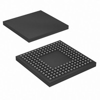
XR17V358IB176-F Exar Corporation, XR17V358IB176-F Datasheet - Page 19

XR17V358IB176-F
Manufacturer Part Number
XR17V358IB176-F
Description
IC UART PCIE OCTAL 176FPBGA
Manufacturer
Exar Corporation
Datasheet
1.XR17V358IB176-F.pdf
(68 pages)
Specifications of XR17V358IB176-F
Number Of Channels
1, UART
Package / Case
176-LFBGA
Features
*
Fifo's
256 Byte
Protocol
RS485
Voltage - Supply
1.2V, 3.3V
With Auto Flow Control
Yes
With Irda Encoder/decoder
Yes
With False Start Bit Detection
Yes
With Modem Control
Yes
Mounting Type
Surface Mount
Data Rate
25 Mbps
Supply Current
120 mA
Maximum Operating Temperature
+ 85 C
Minimum Operating Temperature
- 40 C
Mounting Style
SMD/SMT
Operating Supply Voltage
3.3 V
No. Of Channels
8
Uart Features
Tx/Rx FIFO Counters
Supply Voltage Range
3V To 3.6V
Operating Temperature Range
-40°C To +85°C
Digital Ic Case Style
BGA
No. Of Pins
176
Rohs Compliant
Yes
Lead Free Status / RoHS Status
Lead free / RoHS Compliant
For Use With
1016-1296 - EVAL BOARD FOR XR17V358-E81016-1295 - EVAL BOARD FOR XR17V358-E41016-1293 - EVAL BOARD FOR XR17V358
Lead Free Status / Rohs Status
Lead free / RoHS Compliant
Other names
1016-1294
Available stocks
Company
Part Number
Manufacturer
Quantity
Price
Company:
Part Number:
XR17V358IB176-F
Manufacturer:
EXAR
Quantity:
1 700
Company:
Part Number:
XR17V358IB176-F
Manufacturer:
Exar Corporation
Quantity:
10 000
Part Number:
XR17V358IB176-F
Manufacturer:
EXAR/艾科嘉
Quantity:
20 000
REV. 1.0.2
The XR17V358 has a 32-bit wide register [INT0, INT1, INT2 and INT3] to provide interrupt information and
supports two interrupt schemes. The first scheme is an 8-bit indicator representing all 8 channels with each bit
representing each channel from 0 to 7. This permits the interrupt service routine to quickly determine which
UART channels need servicing so that it can go to the appropriate UART channel interrupt service routines.
INT0 bit [0] represents the interrupt status for UART channel 0 when its transmitter, receiver, line status, or
modem port status requires service. Other bits in the INT0 register provide indication for the other channels
with bit [7] representing UART channel 7 respectively.
The second scheme provides detail about the source of the interrupts for each UART channel. All the interrupts
are encoded into a 3-bit code. This 3-bit code represents 7 interrupts corresponding to individual UART’s
transmitter, receiver, line status, modem port status. INT1, INT2 and INT3 registers provide the 24-bit interrupt
status for all 8 channels. bits [10:8] representing channel 0 and bits [31:29] representing channel 7
respectively. All 8 channel interrupts status are available with a single DWORD read operation. This feature
allows the host another method to quickly service the interrupts, thus reducing the service interval and host
bandwidth requirement.
Note that the interrupts reported in this register is specific to each UART channel. If there is a global interrupt
such as the wake-up interrupt, timer/counter interrupt or MPIO interrupt, they would be reported in the 3-bit
code for channel 0 in INT1.
All bits start up zero. A special interrupt condition is generated by the V358 upon awakening from sleep after all
eight channels were put to sleep mode earlier. This wake-up interrupt is cleared by a read to the INT0 register.
Figure 4
INT0 [7:0] Channel Interrupt Indicator
0x0088-0x008B
0x008C-0x008F
0x0098-0x009B
0x0080
0x0084-0x0087
0x0090-0x0093
0x0094-0x0097
1.4.1
A
DDRESS
A
DDRESS
Ox098
Ox099
0x09A
0x09B
-
0x0083
shows the 4-byte interrupt register and its make up.
[A7:A0]
The Global Interrupt Registers - INT0, INT1, INT2 and INT3
GLOBAL INTERRUPT REGISTER (DWORD)
T
ANCILLARY1 (read/write)
ABLE
ANCILLARY2 (read-only)
T
INTERRUPT (read-only)
ABLE
INT3 [31:24]
TIMER (read/write)
MPIO1 (read/write)
MPIO2 (read/write)
MPIO3 (read/write)
MPIOSEL[15:8]
MPIOINV[15:8]
MPIOOD[15:8]
6: D
R
Reserved
5: D
R
EGISTER
EGISTER
EVICE
EVICE
C
C
ONFIGURATION
ONFIGURATION
Read/Write MPIO[15:8] input polarity select
Read/Write MPIO[15:8] select
Read/Write MPIO[15:8] open-drain output control
INT2 [23:16]
B
MPIOSEL[7:0]
MPIOINT[7:0]
MPIO3T[7:0]
TIMERMSB
YTE
Reserved
SLEEP
INT3
3 [31:24]
R
R
R
EGISTERS SHOWN IN
EAD
19
EGISTERS SHOWN IN
HIGH PERFORMANCE OCTAL PCI EXPRESS UART
/W
RITE
INT1 [15:8]
MPIOLVL[15:8]
B
MPIOOD[15:8]
MPIOINV[7:0]
YTE
TIMERLSB
C
OMMENT
RESET
REGB
INT2
2 [23:16]
[default 0x00-00-00-00]
DWORD
BYTE
MPIOSEL[15:8]
MPIOINT[15:8]
INT0 [7:0]
B
MPIO3T[7:0]
ALIGNMENT
YTE
Reserved
4XMODE
ALIGNMENT
DVID
INT1
1 [15:8]
Bits [15:8] = 0xFF
Bits [15:8] = 0x00
Bits [15:8] = 0x00
RESET STATE
XR17V358
MPIOINV[15:8]
MPIOLVL[7:0]
MPIOOD[7:0]
0x00
B
TIMERCNTL
YTE
8XMODE
DREV
INT0
0 [7:0]


