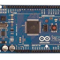
A000047 Arduino, A000047 Datasheet - Page 179
A000047
Manufacturer Part Number
A000047
Description
MCU, MPU & DSP Development Tools Mega2560
Manufacturer
Arduino
Series
-r
Type
MCUr
Specifications of A000047
Processor To Be Evaluated
ATmega2560
Interface Type
USB, I2C, SPI
Dimensions
4 in x 2.1 in
Operating Supply Voltage
5 V
Contents
Board
Lead Free Status / RoHS Status
Lead free / RoHS Compliant
For Use With/related Products
ATmega2560


19.4.4
2549M–AVR–09/10
Phase Correct PWM Mode
in a constantly high or low output (depending on the polarity of the output set by the COM2A1:0
bits).
A frequency (with 50% duty cycle) waveform output in fast PWM mode can be achieved by set-
ting OC2x to toggle its logical level on each compare match (COM2x1:0 = 1). The waveform
generated will have a maximum frequency of f
ture is similar to the OC2A toggle in CTC mode, except the double buffer feature of the Output
Compare unit is enabled in the fast PWM mode.
The phase correct PWM mode (WGM22:0 = 1 or 5) provides a high resolution phase correct
PWM waveform generation option. The phase correct PWM mode is based on a dual-slope
operation. The counter counts repeatedly from BOTTOM to TOP and then from TOP to BOT-
TOM. TOP is defined as 0xFF when WGM22:0 = 1, and OCR2A when MGM22:0 = 5. In non-
inverting Compare Output mode, the Output Compare (OC2x) is cleared on the compare match
between TCNT2 and OCR2x while upcounting, and set on the compare match while downcount-
ing. In inverting Output Compare mode, the operation is inverted. The dual-slope operation has
lower maximum operation frequency than single slope operation. However, due to the symmet-
ric feature of the dual-slope PWM modes, these modes are preferred for motor control
applications.
In phase correct PWM mode the counter is incremented until the counter value matches TOP.
When the counter reaches TOP, it changes the count direction. The TCNT2 value will be equal
to TOP for one timer clock cycle. The timing diagram for the phase correct PWM mode is shown
on
the dual-slope operation. The diagram includes non-inverted and inverted PWM outputs. The
small horizontal line marks on the TCNT2 slopes represent compare matches between OCR2x
and TCNT2.
Figure 19-5. Phase Correct PWM Mode, Timing Diagram
Figure
TCNTn
OCnx
OCnx
Period
19-5. The TCNT2 value is in the timing diagram shown as a histogram for illustrating
1
ATmega640/1280/1281/2560/2561
2
oc2
= f
clk_I/O
/2 when OCR2A is set to zero. This fea-
3
OCnx Interrupt Flag Set
OCRnx Update
TOVn Interrupt Flag Set
(COMnx1:0 = 2)
(COMnx1:0 = 3)
179
Related parts for A000047
Image
Part Number
Description
Manufacturer
Datasheet
Request
R

Part Number:
Description:
Daughter Cards & OEM Boards ARDUINO UNO PROTO PCB REV 3
Manufacturer:
Arduino
Part Number:
Description:
Daughter Cards & OEM Boards ARDUINO SHIELD PROTO KIT REV 3
Manufacturer:
Arduino
Part Number:
Description:
Daughter Cards & OEM Boards ARDUINO MEGA PROTO KIT REV 3
Manufacturer:
Arduino
Part Number:
Description:
Daughter Cards & OEM Boards ARDUINO MEGA PROTO PCB REV 3
Manufacturer:
Arduino
Part Number:
Description:
Development Boards & Kits - AVR ARDUINO STARTER KIT W/ UNO REV3
Manufacturer:
Arduino
Part Number:
Description:
RF Development Tools ARDUINO SHIELD WIRELESS PROTO
Manufacturer:
Arduino
Datasheet:
Part Number:
Description:
RF Development Tools ARDUINO SHIELD WIRELESS WITH SD
Manufacturer:
Arduino
Datasheet:

Part Number:
Description:
Development Software Getting started w/Arduino
Manufacturer:
Arduino

Part Number:
Description:
Ethernet Modules & Development Tools Ethernet Shield for Arduino
Manufacturer:
Arduino

Part Number:
Description:
MCU, MPU & DSP Development Tools LilyPad Arduino Main Board
Manufacturer:
Arduino

Part Number:
Description:
ARDUINO NANO Board
Manufacturer:
Arduino
Datasheet:
Part Number:
Description:
Ethernet Modules & Development Tools ETHERNET SHEILD PoE FOR ARDUINO
Manufacturer:
Arduino
Datasheet:

Part Number:
Description:
ATMEGA328 MCU IC W/ Arduino UNO Bootloader
Manufacturer:
Arduino
Datasheet:
Part Number:
Description:
Memory Cards MICRO SD CARD 1GB WITH SD ADAPTER
Manufacturer:
Arduino