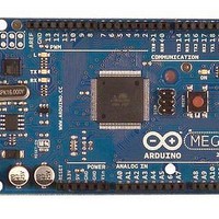
A000047 Arduino, A000047 Datasheet - Page 207
A000047
Manufacturer Part Number
A000047
Description
MCU, MPU & DSP Development Tools Mega2560
Manufacturer
Arduino
Series
-r
Type
MCUr
Specifications of A000047
Processor To Be Evaluated
ATmega2560
Interface Type
USB, I2C, SPI
Dimensions
4 in x 2.1 in
Operating Supply Voltage
5 V
Contents
Board
Lead Free Status / RoHS Status
Lead free / RoHS Compliant
For Use With/related Products
ATmega2560


21.2.1
2549M–AVR–09/10
Internal Clock Generation – The Baud Rate Generator
UCSRnA Register. When using synchronous mode (UMSELn = 1), the Data Direction Register
for the XCKn pin (DDR_XCKn) controls whether the clock source is internal (Master mode) or
external (Slave mode). The XCKn pin is only active when using synchronous mode.
Figure 21-2
Figure 21-2. Clock Generation Logic, Block Diagram
Signal description:
Internal clock generation is used for the asynchronous and the synchronous master modes of
operation. The description in this section refers to
The USART Baud Rate Register (UBRRn) and the down-counter connected to it function as a
programmable prescaler or baud rate generator. The down-counter, running at system clock
(f
the UBRRLn Register is written. A clock is generated each time the counter reaches zero. This
clock is the baud rate generator clock output (= f
baud rate generator clock output by 2, 8 or 16 depending on mode. The baud rate generator out-
put is used directly by the Receiver’s clock and data recovery units. However, the recovery units
use a state machine that uses 2, 8 or 16 states depending on mode set by the state of the
UMSELn, U2Xn and DDR_XCKn bits.
Table 21-1 on page 208
for calculating the UBRRn value for each mode of operation using an internally generated clock
source.
osc
), is loaded with the UBRRn value each time the counter has counted down to zero or when
txclk
rxclk
xcki
xcko
f
OSC
DDR_XCK
XCK
Pin
shows a block diagram of the clock generation logic.
xcko
xcki
OSC
operation.
operation.
Transmitter clock (Internal Signal).
Receiver base clock (Internal Signal).
Input from XCK pin (internal Signal). Used for synchronous slave
Clock output to XCK pin (Internal Signal). Used for synchronous master
XTAL pin frequency (System Clock).
Down-Counter
Prescaling
contains equations for calculating the baud rate (in bits per second) and
Register
UBRR
Sync
ATmega640/1280/1281/2560/2561
UBRR+1
fosc
Detector
UCPOL
Edge
/2
Figure
osc
/(UBRRn+1)). The Transmitter divides the
/4
21-2.
/2
DDR_XCK
U2X
0
1
0
1
0
1
1
0
UMSEL
txclk
rxclk
207
Related parts for A000047
Image
Part Number
Description
Manufacturer
Datasheet
Request
R

Part Number:
Description:
Daughter Cards & OEM Boards ARDUINO UNO PROTO PCB REV 3
Manufacturer:
Arduino
Part Number:
Description:
Daughter Cards & OEM Boards ARDUINO SHIELD PROTO KIT REV 3
Manufacturer:
Arduino
Part Number:
Description:
Daughter Cards & OEM Boards ARDUINO MEGA PROTO KIT REV 3
Manufacturer:
Arduino
Part Number:
Description:
Daughter Cards & OEM Boards ARDUINO MEGA PROTO PCB REV 3
Manufacturer:
Arduino
Part Number:
Description:
Development Boards & Kits - AVR ARDUINO STARTER KIT W/ UNO REV3
Manufacturer:
Arduino
Part Number:
Description:
RF Development Tools ARDUINO SHIELD WIRELESS PROTO
Manufacturer:
Arduino
Datasheet:
Part Number:
Description:
RF Development Tools ARDUINO SHIELD WIRELESS WITH SD
Manufacturer:
Arduino
Datasheet:

Part Number:
Description:
Development Software Getting started w/Arduino
Manufacturer:
Arduino

Part Number:
Description:
Ethernet Modules & Development Tools Ethernet Shield for Arduino
Manufacturer:
Arduino

Part Number:
Description:
MCU, MPU & DSP Development Tools LilyPad Arduino Main Board
Manufacturer:
Arduino

Part Number:
Description:
ARDUINO NANO Board
Manufacturer:
Arduino
Datasheet:
Part Number:
Description:
Ethernet Modules & Development Tools ETHERNET SHEILD PoE FOR ARDUINO
Manufacturer:
Arduino
Datasheet:

Part Number:
Description:
ATMEGA328 MCU IC W/ Arduino UNO Bootloader
Manufacturer:
Arduino
Datasheet:
Part Number:
Description:
Memory Cards MICRO SD CARD 1GB WITH SD ADAPTER
Manufacturer:
Arduino