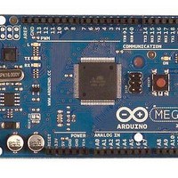
A000047 Arduino, A000047 Datasheet - Page 209
A000047
Manufacturer Part Number
A000047
Description
MCU, MPU & DSP Development Tools Mega2560
Manufacturer
Arduino
Series
-r
Type
MCUr
Specifications of A000047
Processor To Be Evaluated
ATmega2560
Interface Type
USB, I2C, SPI
Dimensions
4 in x 2.1 in
Operating Supply Voltage
5 V
Contents
Board
Lead Free Status / RoHS Status
Lead free / RoHS Compliant
For Use With/related Products
ATmega2560


21.2.4
21.3
2549M–AVR–09/10
Frame Formats
Synchronous Clock Operation
duces a two CPU clock period delay and therefore the maximum external XCKn clock frequency
is limited by the following equation:
Note that f
add some margin to avoid possible loss of data due to frequency variations.
When synchronous mode is used (UMSELn = 1), the XCKn pin will be used as either clock input
(Slave) or clock output (Master). The dependency between the clock edges and data sampling
or data change is the same. The basic principle is that data input (on RxDn) is sampled at the
opposite XCKn clock edge of the edge the data output (TxDn) is changed.
Figure 21-3. Synchronous Mode XCKn Timing.
The UCPOLn bit UCRSC selects which XCKn clock edge is used for data sampling and which is
used for data change. As
rising XCKn edge and sampled at falling XCKn edge. If UCPOLn is set, the data will be changed
at falling XCKn edge and sampled at rising XCKn edge.
A serial frame is defined to be one character of data bits with synchronization bits (start and stop
bits), and optionally a parity bit for error checking. The USART accepts all 30 combinations of
the following as valid frame formats:
•
•
•
•
A frame starts with the start bit followed by the least significant data bit. Then the next data bits,
up to a total of nine, are succeeding, ending with the most significant bit. If enabled, the parity bit
is inserted after the data bits, before the stop bits. When a complete frame is transmitted, it can
be directly followed by a new frame, or the communication line can be set to an idle (high) state.
Figure 21-4 on page 210
brackets are optional.
1 start bit.
5, 6, 7, 8, or 9 data bits.
no, even or odd parity bit.
1 or 2 stop bits.
UCPOL = 1
UCPOL = 0
osc
depends on the stability of the system clock source. It is therefore recommended to
RxD / TxD
RxD / TxD
XCK
XCK
Figure 21-3
illustrates the possible combinations of the frame formats. Bits inside
ATmega640/1280/1281/2560/2561
shows, when UCPOLn is zero the data will be changed at
f
XCK
<
f
---------- -
OSC
4
Sample
Sample
209
Related parts for A000047
Image
Part Number
Description
Manufacturer
Datasheet
Request
R

Part Number:
Description:
Daughter Cards & OEM Boards ARDUINO UNO PROTO PCB REV 3
Manufacturer:
Arduino
Part Number:
Description:
Daughter Cards & OEM Boards ARDUINO SHIELD PROTO KIT REV 3
Manufacturer:
Arduino
Part Number:
Description:
Daughter Cards & OEM Boards ARDUINO MEGA PROTO KIT REV 3
Manufacturer:
Arduino
Part Number:
Description:
Daughter Cards & OEM Boards ARDUINO MEGA PROTO PCB REV 3
Manufacturer:
Arduino
Part Number:
Description:
Development Boards & Kits - AVR ARDUINO STARTER KIT W/ UNO REV3
Manufacturer:
Arduino
Part Number:
Description:
RF Development Tools ARDUINO SHIELD WIRELESS PROTO
Manufacturer:
Arduino
Datasheet:
Part Number:
Description:
RF Development Tools ARDUINO SHIELD WIRELESS WITH SD
Manufacturer:
Arduino
Datasheet:

Part Number:
Description:
Development Software Getting started w/Arduino
Manufacturer:
Arduino

Part Number:
Description:
Ethernet Modules & Development Tools Ethernet Shield for Arduino
Manufacturer:
Arduino

Part Number:
Description:
MCU, MPU & DSP Development Tools LilyPad Arduino Main Board
Manufacturer:
Arduino

Part Number:
Description:
ARDUINO NANO Board
Manufacturer:
Arduino
Datasheet:
Part Number:
Description:
Ethernet Modules & Development Tools ETHERNET SHEILD PoE FOR ARDUINO
Manufacturer:
Arduino
Datasheet:

Part Number:
Description:
ATMEGA328 MCU IC W/ Arduino UNO Bootloader
Manufacturer:
Arduino
Datasheet:
Part Number:
Description:
Memory Cards MICRO SD CARD 1GB WITH SD ADAPTER
Manufacturer:
Arduino