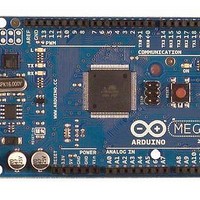
A000047 Arduino, A000047 Datasheet - Page 37
A000047
Manufacturer Part Number
A000047
Description
MCU, MPU & DSP Development Tools Mega2560
Manufacturer
Arduino
Series
-r
Type
MCUr
Specifications of A000047
Processor To Be Evaluated
ATmega2560
Interface Type
USB, I2C, SPI
Dimensions
4 in x 2.1 in
Operating Supply Voltage
5 V
Contents
Board
Lead Free Status / RoHS Status
Lead free / RoHS Compliant
For Use With/related Products
ATmega2560


8.3
8.3.1
8.3.2
8.3.3
8.4
8.4.1
2549M–AVR–09/10
General Purpose registers
External Memory registers
GPIOR2 – General Purpose I/O Register 2
GPIOR1 – General Purpose I/O Register 1
GPIOR0 – General Purpose I/O Register 0
XMCRA – External Memory Control Register A
• Bit 0 – EERE: EEPROM Read Enable
The EEPROM Read Enable Signal EERE is the read strobe to the EEPROM. When the correct
address is set up in the EEAR Register, the EERE bit must be written to a logic one to trigger the
EEPROM read. The EEPROM read access takes one instruction, and the requested data is
available immediately. When the EEPROM is read, the CPU is halted for four cycles before the
next instruction is executed.
The user should poll the EEPE bit before starting the read operation. If a write operation is in
progress, it is neither possible to read the EEPROM, nor to change the EEAR Register.
• Bit 7 – SRE: External SRAM/XMEM Enable
Writing SRE to one enables the External Memory Interface.The pin functions AD7:0, A15:8,
ALE, WR, and RD are activated as the alternate pin functions. The SRE bit overrides any pin
direction settings in the respective data direction registers. Writing SRE to zero, disables the
External Memory Interface and the normal pin and data direction settings are used.
• Bit 6:4 – SRL2:0: Wait-state Sector Limit
It is possible to configure different wait-states for different External Memory addresses. The
external memory address space can be divided in two sectors that have separate wait-state bits.
The SRL2, SRL1, and SRL0 bits select the split of the sectors, see
Bit
0x2B (0x4B)
Read/Write
Initial Value
Bit
0x2A (0x4A)
Read/Write
Initial Value
Bit
0x1E (0x3E)
Read/Write
Initial Value
Bit
“(0x74)”
Read/Write
Initial Value
MSB
MSB
MSB
R/W
R/W
R/W
SRE
R/W
7
0
7
0
7
0
7
0
SRL2
R/W
R/W
R/W
R/W
6
0
6
0
6
0
6
0
ATmega640/1280/1281/2560/2561
SRL1
R/W
R/W
R/W
R/W
5
0
5
0
5
0
5
0
SRL0
R/W
R/W
R/W
R/W
4
0
4
0
4
0
4
0
SRW11
R/W
R/W
R/W
R/W
3
0
3
0
3
0
3
0
SRW10
R/W
R/W
R/W
R/W
2
0
2
0
2
0
2
0
Table 8-2 on page 38
SRW01
R/W
R/W
R/W
R/W
1
0
1
0
1
0
1
0
SRW00
LSB
LSB
LSB
R/W
R/W
R/W
R/W
0
0
0
0
0
0
0
0
GPIOR2
GPIOR1
GPIOR0
XMCRA
and
37
Related parts for A000047
Image
Part Number
Description
Manufacturer
Datasheet
Request
R

Part Number:
Description:
Daughter Cards & OEM Boards ARDUINO UNO PROTO PCB REV 3
Manufacturer:
Arduino
Part Number:
Description:
Daughter Cards & OEM Boards ARDUINO SHIELD PROTO KIT REV 3
Manufacturer:
Arduino
Part Number:
Description:
Daughter Cards & OEM Boards ARDUINO MEGA PROTO KIT REV 3
Manufacturer:
Arduino
Part Number:
Description:
Daughter Cards & OEM Boards ARDUINO MEGA PROTO PCB REV 3
Manufacturer:
Arduino
Part Number:
Description:
Development Boards & Kits - AVR ARDUINO STARTER KIT W/ UNO REV3
Manufacturer:
Arduino
Part Number:
Description:
RF Development Tools ARDUINO SHIELD WIRELESS PROTO
Manufacturer:
Arduino
Datasheet:
Part Number:
Description:
RF Development Tools ARDUINO SHIELD WIRELESS WITH SD
Manufacturer:
Arduino
Datasheet:

Part Number:
Description:
Development Software Getting started w/Arduino
Manufacturer:
Arduino

Part Number:
Description:
Ethernet Modules & Development Tools Ethernet Shield for Arduino
Manufacturer:
Arduino

Part Number:
Description:
MCU, MPU & DSP Development Tools LilyPad Arduino Main Board
Manufacturer:
Arduino

Part Number:
Description:
ARDUINO NANO Board
Manufacturer:
Arduino
Datasheet:
Part Number:
Description:
Ethernet Modules & Development Tools ETHERNET SHEILD PoE FOR ARDUINO
Manufacturer:
Arduino
Datasheet:

Part Number:
Description:
ATMEGA328 MCU IC W/ Arduino UNO Bootloader
Manufacturer:
Arduino
Datasheet:
Part Number:
Description:
Memory Cards MICRO SD CARD 1GB WITH SD ADAPTER
Manufacturer:
Arduino