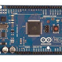
A000047 Arduino, A000047 Datasheet - Page 282
A000047
Manufacturer Part Number
A000047
Description
MCU, MPU & DSP Development Tools Mega2560
Manufacturer
Arduino
Series
-r
Type
MCUr
Specifications of A000047
Processor To Be Evaluated
ATmega2560
Interface Type
USB, I2C, SPI
Dimensions
4 in x 2.1 in
Operating Supply Voltage
5 V
Contents
Board
Lead Free Status / RoHS Status
Lead free / RoHS Compliant
For Use With/related Products
ATmega2560


25.5
25.5.1
2549M–AVR–09/10
Changing Channel or Reference Selection
ADC Input Channels
The MUXn and REFS1:0 bits in the ADMUX Register are single buffered through a temporary
register to which the CPU has random access. This ensures that the channels and reference
selection only takes place at a safe point during the conversion. The channel and reference
selection is continuously updated until a conversion is started. Once the conversion starts, the
channel and reference selection is locked to ensure a sufficient sampling time for the ADC. Con-
tinuous updating resumes in the last ADC clock cycle before the conversion completes (ADIF in
ADCSRA is set). Note that the conversion starts on the following rising ADC clock edge after
ADSC is written. The user is thus advised not to write new channel or reference selection values
to ADMUX until one ADC clock cycle after ADSC is written.
If Auto Triggering is used, the exact time of the triggering event can be indeterministic. Special
care must be taken when updating the ADMUX Register, in order to control which conversion
will be affected by the new settings.
If both ADATE and ADEN is written to one, an interrupt event can occur at any time. If the
ADMUX Register is changed in this period, the user cannot tell if the next conversion is based
on the old or the new settings. ADMUX can be safely updated in the following ways:
When updating ADMUX in one of these conditions, the new settings will affect the next ADC
conversion.
Special care should be taken when changing differential channels. Once a differential channel
has been selected, the stage may take as much as 125 µs to stabilize to the new value. Thus
conversions should not be started within the first 125 µs after selecting a new differential chan-
nel. Alternatively, conversion results obtained within this period should be discarded.
The same settling time should be observed for the first differential conversion after changing
ADC reference (by changing the REFS1:0 bits in ADMUX).
When changing channel selections, the user should observe the following guidelines to ensure
that the correct channel is selected:
In Single Conversion mode, always select the channel before starting the conversion. The chan-
nel selection may be changed one ADC clock cycle after writing one to ADSC. However, the
simplest method is to wait for the conversion to complete before changing the channel selection.
In Free Running mode, always select the channel before starting the first conversion. The chan-
nel selection may be changed one ADC clock cycle after writing one to ADSC. However, the
simplest method is to wait for the first conversion to complete, and then change the channel
selection. Since the next conversion has already started automatically, the next result will reflect
the previous channel selection. Subsequent conversions will reflect the new channel selection.
When switching to a differential gain channel, the first conversion result may have a poor accu-
racy due to the required settling time for the automatic offset cancellation circuitry. The user
should preferably disregard the first conversion result.
1. When ADATE or ADEN is cleared.
2. During conversion, minimum one ADC clock cycle after the trigger event.
3. After a conversion, before the Interrupt Flag used as trigger source is cleared.
ATmega640/1280/1281/2560/2561
282
Related parts for A000047
Image
Part Number
Description
Manufacturer
Datasheet
Request
R

Part Number:
Description:
Daughter Cards & OEM Boards ARDUINO UNO PROTO PCB REV 3
Manufacturer:
Arduino
Part Number:
Description:
Daughter Cards & OEM Boards ARDUINO SHIELD PROTO KIT REV 3
Manufacturer:
Arduino
Part Number:
Description:
Daughter Cards & OEM Boards ARDUINO MEGA PROTO KIT REV 3
Manufacturer:
Arduino
Part Number:
Description:
Daughter Cards & OEM Boards ARDUINO MEGA PROTO PCB REV 3
Manufacturer:
Arduino
Part Number:
Description:
Development Boards & Kits - AVR ARDUINO STARTER KIT W/ UNO REV3
Manufacturer:
Arduino
Part Number:
Description:
RF Development Tools ARDUINO SHIELD WIRELESS PROTO
Manufacturer:
Arduino
Datasheet:
Part Number:
Description:
RF Development Tools ARDUINO SHIELD WIRELESS WITH SD
Manufacturer:
Arduino
Datasheet:

Part Number:
Description:
Development Software Getting started w/Arduino
Manufacturer:
Arduino

Part Number:
Description:
Ethernet Modules & Development Tools Ethernet Shield for Arduino
Manufacturer:
Arduino

Part Number:
Description:
MCU, MPU & DSP Development Tools LilyPad Arduino Main Board
Manufacturer:
Arduino

Part Number:
Description:
ARDUINO NANO Board
Manufacturer:
Arduino
Datasheet:
Part Number:
Description:
Ethernet Modules & Development Tools ETHERNET SHEILD PoE FOR ARDUINO
Manufacturer:
Arduino
Datasheet:

Part Number:
Description:
ATMEGA328 MCU IC W/ Arduino UNO Bootloader
Manufacturer:
Arduino
Datasheet:
Part Number:
Description:
Memory Cards MICRO SD CARD 1GB WITH SD ADAPTER
Manufacturer:
Arduino