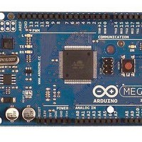
A000047 Arduino, A000047 Datasheet - Page 50
A000047
Manufacturer Part Number
A000047
Description
MCU, MPU & DSP Development Tools Mega2560
Manufacturer
Arduino
Series
-r
Type
MCUr
Specifications of A000047
Processor To Be Evaluated
ATmega2560
Interface Type
USB, I2C, SPI
Dimensions
4 in x 2.1 in
Operating Supply Voltage
5 V
Contents
Board
Lead Free Status / RoHS Status
Lead free / RoHS Compliant
For Use With/related Products
ATmega2560


9.13
9.13.1
9.13.2
2549M–AVR–09/10
Register Description
OSCCAL – Oscillator Calibration Register
CLKPR – Clock Prescale Register
• Bits 7:0 – CAL7:0: Oscillator Calibration Value
The Oscillator Calibration Register is used to trim the Calibrated Internal RC Oscillator to
remove process variations from the oscillator frequency. A pre-programmed calibration value is
automatically written to this register during chip reset, giving the Factory calibrated frequency as
specified in
the oscillator frequency. The oscillator can be calibrated to frequencies as specified in
1 on page
Note that this oscillator is used to time EEPROM and Flash write accesses, and these write
times will be affected accordingly. If the EEPROM or Flash are written, do not calibrate to more
than 8.8 MHz. Otherwise, the EEPROM or Flash write may fail.
The CAL7 bit determines the range of operation for the oscillator. Setting this bit to 0 gives the
lowest frequency range, setting this bit to 1 gives the highest frequency range. The two fre-
quency ranges are overlapping, in other words a setting of OSCCAL = 0x7F gives a higher
frequency than OSCCAL = 0x80.
The CAL6..0 bits are used to tune the frequency within the selected range. A setting of 0x00
gives the lowest frequency in that range, and a setting of 0x7F gives the highest frequency in the
range.
• Bit 7 – CLKPCE: Clock Prescaler Change Enable
The CLKPCE bit must be written to logic one to enable change of the CLKPS bits. The CLKPCE
bit is only updated when the other bits in CLKPR are simultaneously written to zero. CLKPCE is
cleared by hardware four cycles after it is written or when CLKPS bits are written. Rewriting the
CLKPCE bit within this time-out period does neither extend the time-out period, nor clear the
CLKPCE bit.
• Bits 3:0 – CLKPS3:0: Clock Prescaler Select Bits 3 - 0
These bits define the division factor between the selected clock source and the internal system
clock. These bits can be written run-time to vary the clock frequency to suit the application
requirements. As the divider divides the master clock input to the MCU, the speed of all synchro-
nous peripherals is reduced when a division factor is used. The division factors are given in
Table 9-15 on page
The CKDIV8 Fuse determines the initial value of the CLKPS bits. If CKDIV8 is unprogrammed,
the CLKPS bits will be reset to “0000”. If CKDIV8 is programmed, CLKPS bits are reset to
“0011”, giving a division factor of 8 at start up. This feature should be used if the selected clock
Bit
(0x66)
Read/Write
Initial Value
Bit
(0x61)
Read/Write
Initial Value
371. Calibration outside that range is not guaranteed.
Table 30-1 on page
CLKPCE
CAL7
R/W
R/W
7
7
0
51.
CAL6
R/W
6
R
6
–
0
ATmega640/1280/1281/2560/2561
371. The application software can write this register to change
CAL5
R/W
5
R
5
–
0
Device Specific Calibration Value
CAL4
R/W
4
R
4
–
0
CLKPS3
CAL3
R/W
R/W
3
3
CLKPS2
CAL2
See Bit Description
R/W
R/W
2
2
CLKPS1
CAL1
R/W
R/W
1
1
CLKPS0
CAL0
R/W
R/W
0
0
Table 30-
OSCCAL
CLKPR
50
Related parts for A000047
Image
Part Number
Description
Manufacturer
Datasheet
Request
R

Part Number:
Description:
Daughter Cards & OEM Boards ARDUINO UNO PROTO PCB REV 3
Manufacturer:
Arduino
Part Number:
Description:
Daughter Cards & OEM Boards ARDUINO SHIELD PROTO KIT REV 3
Manufacturer:
Arduino
Part Number:
Description:
Daughter Cards & OEM Boards ARDUINO MEGA PROTO KIT REV 3
Manufacturer:
Arduino
Part Number:
Description:
Daughter Cards & OEM Boards ARDUINO MEGA PROTO PCB REV 3
Manufacturer:
Arduino
Part Number:
Description:
Development Boards & Kits - AVR ARDUINO STARTER KIT W/ UNO REV3
Manufacturer:
Arduino
Part Number:
Description:
RF Development Tools ARDUINO SHIELD WIRELESS PROTO
Manufacturer:
Arduino
Datasheet:
Part Number:
Description:
RF Development Tools ARDUINO SHIELD WIRELESS WITH SD
Manufacturer:
Arduino
Datasheet:

Part Number:
Description:
Development Software Getting started w/Arduino
Manufacturer:
Arduino

Part Number:
Description:
Ethernet Modules & Development Tools Ethernet Shield for Arduino
Manufacturer:
Arduino

Part Number:
Description:
MCU, MPU & DSP Development Tools LilyPad Arduino Main Board
Manufacturer:
Arduino

Part Number:
Description:
ARDUINO NANO Board
Manufacturer:
Arduino
Datasheet:
Part Number:
Description:
Ethernet Modules & Development Tools ETHERNET SHEILD PoE FOR ARDUINO
Manufacturer:
Arduino
Datasheet:

Part Number:
Description:
ATMEGA328 MCU IC W/ Arduino UNO Bootloader
Manufacturer:
Arduino
Datasheet:
Part Number:
Description:
Memory Cards MICRO SD CARD 1GB WITH SD ADAPTER
Manufacturer:
Arduino