A000047 Arduino, A000047 Datasheet - Page 284
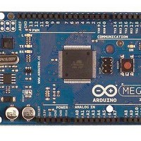
A000047
Manufacturer Part Number
A000047
Description
MCU, MPU & DSP Development Tools Mega2560
Manufacturer
Arduino
Series
-r
Type
MCUr
Specifications of A000047
Processor To Be Evaluated
ATmega2560
Interface Type
USB, I2C, SPI
Dimensions
4 in x 2.1 in
Operating Supply Voltage
5 V
Contents
Board
Lead Free Status / RoHS Status
Lead free / RoHS Compliant
For Use With/related Products
ATmega2560


25.6.1
25.6.2
2549M–AVR–09/10
Analog Input Circuitry
Analog Noise Canceling Techniques
The analog input circuitry for single ended channels is illustrated in Figure 25-8. An analog
source applied to ADCn is subjected to the pin capacitance and input leakage of that pin, regard-
less of whether that channel is selected as input for the ADC. When the channel is selected, the
source must drive the S/H capacitor through the series resistance (combined resistance in the
input path).
The ADC is optimized for analog signals with an output impedance of approximately 10 kΩ or
less. If such a source is used, the sampling time will be negligible. If a source with higher imped-
ance is used, the sampling time will depend on how long time the source needs to charge the
S/H capacitor, which can vary widely. The user is recommended to only use low impedant
sources with slowly varying signals, since this minimizes the required charge transfer to the S/H
capacitor.
Signal components higher than the Nyquist frequency (f
kind of channels, to avoid distortion from unpredictable signal convolution. The user is advised
to remove high frequency components with a low-pass filter before applying the signals as
inputs to the ADC.
Figure 25-8. Analog Input Circuitry
Digital circuitry inside and outside the device generates EMI which might affect the accuracy of
analog measurements. If conversion accuracy is critical, the noise level can be reduced by
applying the following techniques:
1. Keep analog signal paths as short as possible. Make sure analog tracks run over the
2. The AVCC pin on the device should be connected to the digital V
3. Use the ADC noise canceler function to reduce induced noise from the CPU.
4. If any ADC port pins are used as digital outputs, it is essential that these do not
ground plane, and keep them well away from high-speed switching digital tracks.
via an LC network as shown in
switch while a conversion is in progress.
ADCn
I
IH
ATmega640/1280/1281/2560/2561
I
IL
Figure 25-9 on page
1..100 kΩ
ADC
/2) should not be present for either
285.
C
S/H
= 14 pF
CC
supply voltage
V
CC
/2
284
Related parts for A000047
Image
Part Number
Description
Manufacturer
Datasheet
Request
R

Part Number:
Description:
Daughter Cards & OEM Boards ARDUINO UNO PROTO PCB REV 3
Manufacturer:
Arduino
Part Number:
Description:
Daughter Cards & OEM Boards ARDUINO SHIELD PROTO KIT REV 3
Manufacturer:
Arduino
Part Number:
Description:
Daughter Cards & OEM Boards ARDUINO MEGA PROTO KIT REV 3
Manufacturer:
Arduino
Part Number:
Description:
Daughter Cards & OEM Boards ARDUINO MEGA PROTO PCB REV 3
Manufacturer:
Arduino
Part Number:
Description:
Development Boards & Kits - AVR ARDUINO STARTER KIT W/ UNO REV3
Manufacturer:
Arduino
Part Number:
Description:
RF Development Tools ARDUINO SHIELD WIRELESS PROTO
Manufacturer:
Arduino
Datasheet:
Part Number:
Description:
RF Development Tools ARDUINO SHIELD WIRELESS WITH SD
Manufacturer:
Arduino
Datasheet:

Part Number:
Description:
Development Software Getting started w/Arduino
Manufacturer:
Arduino

Part Number:
Description:
Ethernet Modules & Development Tools Ethernet Shield for Arduino
Manufacturer:
Arduino

Part Number:
Description:
MCU, MPU & DSP Development Tools LilyPad Arduino Main Board
Manufacturer:
Arduino

Part Number:
Description:
ARDUINO NANO Board
Manufacturer:
Arduino
Datasheet:
Part Number:
Description:
Ethernet Modules & Development Tools ETHERNET SHEILD PoE FOR ARDUINO
Manufacturer:
Arduino
Datasheet:

Part Number:
Description:
ATMEGA328 MCU IC W/ Arduino UNO Bootloader
Manufacturer:
Arduino
Datasheet:
Part Number:
Description:
Memory Cards MICRO SD CARD 1GB WITH SD ADAPTER
Manufacturer:
Arduino