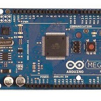
A000047 Arduino, A000047 Datasheet - Page 89
A000047
Manufacturer Part Number
A000047
Description
MCU, MPU & DSP Development Tools Mega2560
Manufacturer
Arduino
Series
-r
Type
MCUr
Specifications of A000047
Processor To Be Evaluated
ATmega2560
Interface Type
USB, I2C, SPI
Dimensions
4 in x 2.1 in
Operating Supply Voltage
5 V
Contents
Board
Lead Free Status / RoHS Status
Lead free / RoHS Compliant
For Use With/related Products
ATmega2560


12.3.6
2549M–AVR–09/10
Alternate Functions of Port F
The Port F has an alternate function as analog input for the ADC as shown in
some Port F pins are configured as outputs, it is essential that these do not switch when a con-
version is in progress. This might corrupt the result of the conversion. If the JTAG interface is
enabled, the pull-up resistors on pins PF7(TDI), PF5(TMS), and PF4(TCK) will be activated even
if a Reset occurs.
Table 12-18. Port F Pins Alternate Functions
• TDI, ADC7 – Port F, Bit 7
ADC7, Analog to Digital Converter, Channel 7.
TDI, JTAG Test Data In: Serial input data to be shifted in to the Instruction Register or Data Reg-
ister (scan chains). When the JTAG interface is enabled, this pin can not be used as an I/O pin.
• TDO, ADC6 – Port F, Bit 6
ADC6, Analog to Digital Converter, Channel 6.
TDO, JTAG Test Data Out: Serial output data from Instruction Register or Data Register. When
the JTAG interface is enabled, this pin can not be used as an I/O pin.
The TDO pin is tri-stated unless TAP states that shift out data are entered.
• TMS, ADC5 – Port F, Bit 5
ADC5, Analog to Digital Converter, Channel 5.
TMS, JTAG Test Mode Select: This pin is used for navigating through the TAP-controller state
machine. When the JTAG interface is enabled, this pin can not be used as an I/O pin.
• TCK, ADC4 – Port F, Bit 4
ADC4, Analog to Digital Converter, Channel 4.
TCK, JTAG Test Clock: JTAG operation is synchronous to TCK. When the JTAG interface is
enabled, this pin can not be used as an I/O pin.
• ADC3 – ADC0 – Port F, Bit 3:0
Analog to Digital Converter, Channel 3:0.
Port Pin
PF7
PF6
PF5
PF4
PF3
PF2
PF1
PF0
ADC5/TMS (ADC input channel 5 or JTAG Test Mode Select)
ADC6/TDO (ADC input channel 6 or JTAG Test Data Output)
ADC7/TDI (ADC input channel 7 or JTAG Test Data Input)
ADC4/TCK (ADC input channel 4 or JTAG Test ClocK)
ATmega640/1280/1281/2560/2561
ADC3 (ADC input channel 3)
ADC2 (ADC input channel 2)
ADC1 (ADC input channel 1)
ADC0 (ADC input channel 0)
Alternate Function
Table
12-18. If
89
Related parts for A000047
Image
Part Number
Description
Manufacturer
Datasheet
Request
R

Part Number:
Description:
Daughter Cards & OEM Boards ARDUINO UNO PROTO PCB REV 3
Manufacturer:
Arduino
Part Number:
Description:
Daughter Cards & OEM Boards ARDUINO SHIELD PROTO KIT REV 3
Manufacturer:
Arduino
Part Number:
Description:
Daughter Cards & OEM Boards ARDUINO MEGA PROTO KIT REV 3
Manufacturer:
Arduino
Part Number:
Description:
Daughter Cards & OEM Boards ARDUINO MEGA PROTO PCB REV 3
Manufacturer:
Arduino
Part Number:
Description:
Development Boards & Kits - AVR ARDUINO STARTER KIT W/ UNO REV3
Manufacturer:
Arduino
Part Number:
Description:
RF Development Tools ARDUINO SHIELD WIRELESS PROTO
Manufacturer:
Arduino
Datasheet:
Part Number:
Description:
RF Development Tools ARDUINO SHIELD WIRELESS WITH SD
Manufacturer:
Arduino
Datasheet:

Part Number:
Description:
Development Software Getting started w/Arduino
Manufacturer:
Arduino

Part Number:
Description:
Ethernet Modules & Development Tools Ethernet Shield for Arduino
Manufacturer:
Arduino

Part Number:
Description:
MCU, MPU & DSP Development Tools LilyPad Arduino Main Board
Manufacturer:
Arduino

Part Number:
Description:
ARDUINO NANO Board
Manufacturer:
Arduino
Datasheet:
Part Number:
Description:
Ethernet Modules & Development Tools ETHERNET SHEILD PoE FOR ARDUINO
Manufacturer:
Arduino
Datasheet:

Part Number:
Description:
ATMEGA328 MCU IC W/ Arduino UNO Bootloader
Manufacturer:
Arduino
Datasheet:
Part Number:
Description:
Memory Cards MICRO SD CARD 1GB WITH SD ADAPTER
Manufacturer:
Arduino