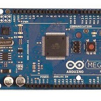
A000047 Arduino, A000047 Datasheet - Page 91
A000047
Manufacturer Part Number
A000047
Description
MCU, MPU & DSP Development Tools Mega2560
Manufacturer
Arduino
Series
-r
Type
MCUr
Specifications of A000047
Processor To Be Evaluated
ATmega2560
Interface Type
USB, I2C, SPI
Dimensions
4 in x 2.1 in
Operating Supply Voltage
5 V
Contents
Board
Lead Free Status / RoHS Status
Lead free / RoHS Compliant
For Use With/related Products
ATmega2560


2549M–AVR–09/10
• OC0B – Port G, Bit 5
OC0B, Output Compare match B output: The PG5 pin can serve as an external output for the
TImer/Counter0 Output Compare. The pin has to be configured as an output (DDG5 set) to
serve this function. The OC0B pin is also the output pin for the PWM mode timer function.
• TOSC1 – Port G, Bit 4
TOSC2, Timer Oscillator pin 1: When the AS2 bit in ASSR is set (one) to enable asynchronous
clocking of Timer/Counter2, pin PG4 is disconnected from the port, and becomes the input of the
inverting Oscillator amplifier. In this mode, a Crystal Oscillator is connected to this pin, and the
pin can not be used as an I/O pin.
• TOSC2 – Port G, Bit 3
TOSC2, Timer Oscillator pin 2: When the AS2 bit in ASSR is set (one) to enable asynchronous
clocking of Timer/Counter2, pin PG3 is disconnected from the port, and becomes the inverting
output of the Oscillator amplifier. In this mode, a Crystal Oscillator is connected to this pin, and
the pin can not be used as an I/O pin.
• ALE – Port G, Bit 2
ALE is the external data memory Address Latch Enable signal.
• RD – Port G, Bit 1
RD is the external data memory read control strobe.
• WR – Port G, Bit 0
WR is the external data memory write control strobe.
Table 12-22 on page 91
the overriding signals shown in
Table 12-22. Overriding Signals for Alternate Functions in PG5:PG4
Signal Name
DIEOE
DIEOV
PUOE
DDOE
DDOV
PUOV
PVOE
PVOV
PTOE
AIO
DI
and
—
–
–
–
–
–
–
–
–
–
–
–
Table 12-23 on page 92
Figure 12-5 on page
ATmega640/1280/1281/2560/2561
—
–
–
–
–
–
–
–
–
–
–
–
76.
relates the alternate functions of Port G to
OC0B Enable
PG5/OC0B
OC0B
–
–
–
–
–
–
–
–
–
T/C2 OSC INPUT
PG4/TOSC1
EXCLK
AS2
AS2
AS2
0
0
0
0
–
–
91
Related parts for A000047
Image
Part Number
Description
Manufacturer
Datasheet
Request
R

Part Number:
Description:
Daughter Cards & OEM Boards ARDUINO UNO PROTO PCB REV 3
Manufacturer:
Arduino
Part Number:
Description:
Daughter Cards & OEM Boards ARDUINO SHIELD PROTO KIT REV 3
Manufacturer:
Arduino
Part Number:
Description:
Daughter Cards & OEM Boards ARDUINO MEGA PROTO KIT REV 3
Manufacturer:
Arduino
Part Number:
Description:
Daughter Cards & OEM Boards ARDUINO MEGA PROTO PCB REV 3
Manufacturer:
Arduino
Part Number:
Description:
Development Boards & Kits - AVR ARDUINO STARTER KIT W/ UNO REV3
Manufacturer:
Arduino
Part Number:
Description:
RF Development Tools ARDUINO SHIELD WIRELESS PROTO
Manufacturer:
Arduino
Datasheet:
Part Number:
Description:
RF Development Tools ARDUINO SHIELD WIRELESS WITH SD
Manufacturer:
Arduino
Datasheet:

Part Number:
Description:
Development Software Getting started w/Arduino
Manufacturer:
Arduino

Part Number:
Description:
Ethernet Modules & Development Tools Ethernet Shield for Arduino
Manufacturer:
Arduino

Part Number:
Description:
MCU, MPU & DSP Development Tools LilyPad Arduino Main Board
Manufacturer:
Arduino

Part Number:
Description:
ARDUINO NANO Board
Manufacturer:
Arduino
Datasheet:
Part Number:
Description:
Ethernet Modules & Development Tools ETHERNET SHEILD PoE FOR ARDUINO
Manufacturer:
Arduino
Datasheet:

Part Number:
Description:
ATMEGA328 MCU IC W/ Arduino UNO Bootloader
Manufacturer:
Arduino
Datasheet:
Part Number:
Description:
Memory Cards MICRO SD CARD 1GB WITH SD ADAPTER
Manufacturer:
Arduino